
New Purdue-led consortium assembles the future of semiconductor packaging

“Advanced packaging is the future,” said Ganesh Subbarayan, James G. Dwyer Professor of Mechanical Engineering. “We’ve known for a while that Moore’s Law cannot continue forever.”
Moore’s Law is the rule of thumb that the number of transistors on a computer processor has generally doubled every two years since 1965. But even with the most advanced nanomanufacturing techniques, these chips will soon hit physical limits that will be difficult to overcome — thus the exploration of advanced packaging.
Purdue University has led this effort from the academic side. In 2022, they launched the country’s first comprehensive semiconductor degrees program, with 55 faculty members teaching more than 100 different courses at the graduate and undergraduate level. A year later, Subbarayan brought together the University’s faculty and resources to create the Atalla Institute for Advanced System Integration and Packaging (ASIP). The institute bears the name of John Attala, Purdue Mechanical Engineering graduate and co-inventor of the MOSFET in 1960 which led to the development of the integrated circuit.
Those initiatives are already paying dividends beyond academia. Just this summer, Korean memory chip manufacturer SK hynix broke ground on a $4 billion advanced packaging production facility at Purdue’s Research Park.
To further catalyze these efforts, Subbarayan organized the ASIP Consortium, gathering globally preeminent memory and processor design and fabrication companies, fabless system integrators, equipment vendors, inspection tool developers, materials suppliers, electronic design automation tool companies, and university researchers to progress advanced system integration and packaging solutions for future computing and communication systems. Purdue University hosted the kickoff event in October 2026.
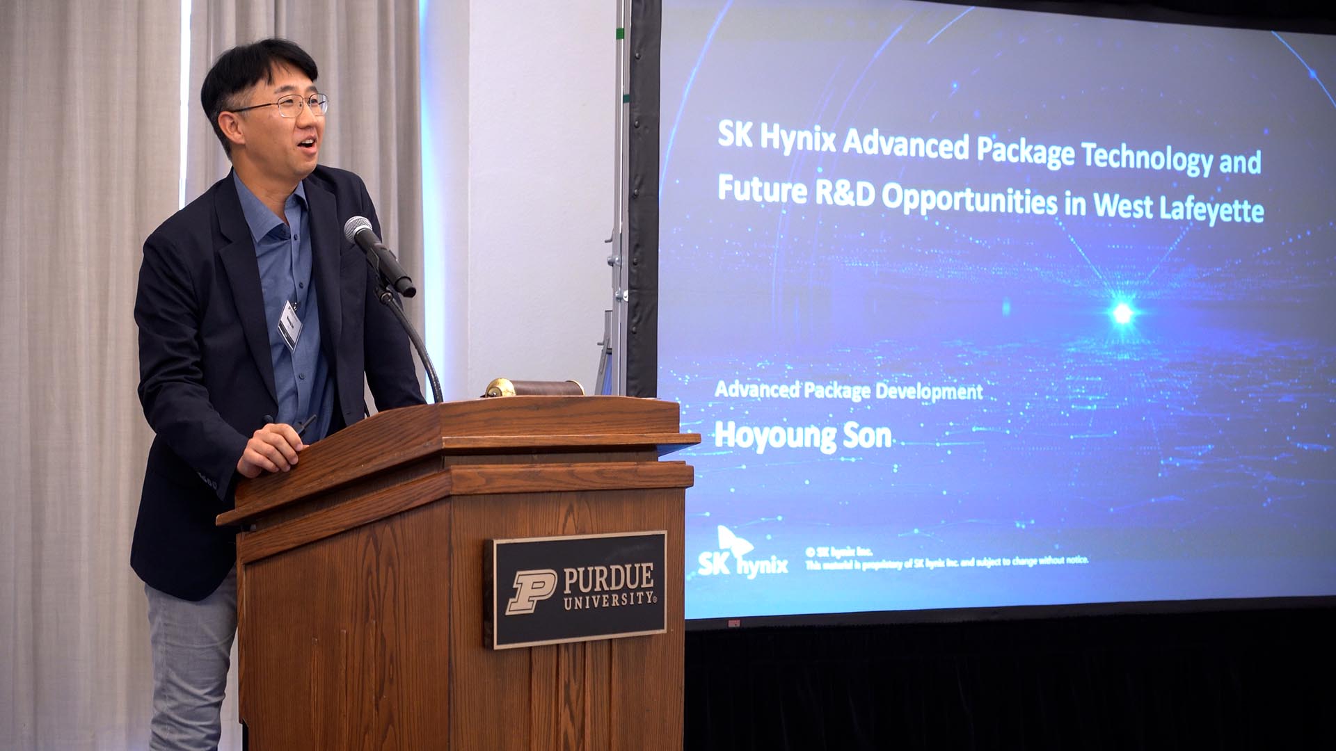
“It was incredible to have all of these people in one place,” Subbarayan said. “We were all excited to learn the technical challenges, but also tackle the logistical challenges of how we can all collaborate and build the pre-competitive research ecosystem.”
Dr. Hoyoung Son, Vice President and Head of Advanced Packaging Development for SK hynix, traveled from Korea to give one of the keynote presentations; another was presented by Dr. Raja Swaminathan, Corporate Vice President of Heterogeneous Integration Technologies at AMD. Other participants included representatives from Amazon, MediaTek, Intel, GlobalFoundries, Hitachi, Sandisk, Lam Research, Applied Materials, Tokyo Electron, ASMPT, NHanced Semiconductors, Resonac, Qnity, JSR Corporation, JX, Dassault Systemes, Cadence Design Systems, Semiconductor Research Corporation, Imec, SEMI, Global Electronics Association, and Sandia National Laboratories.
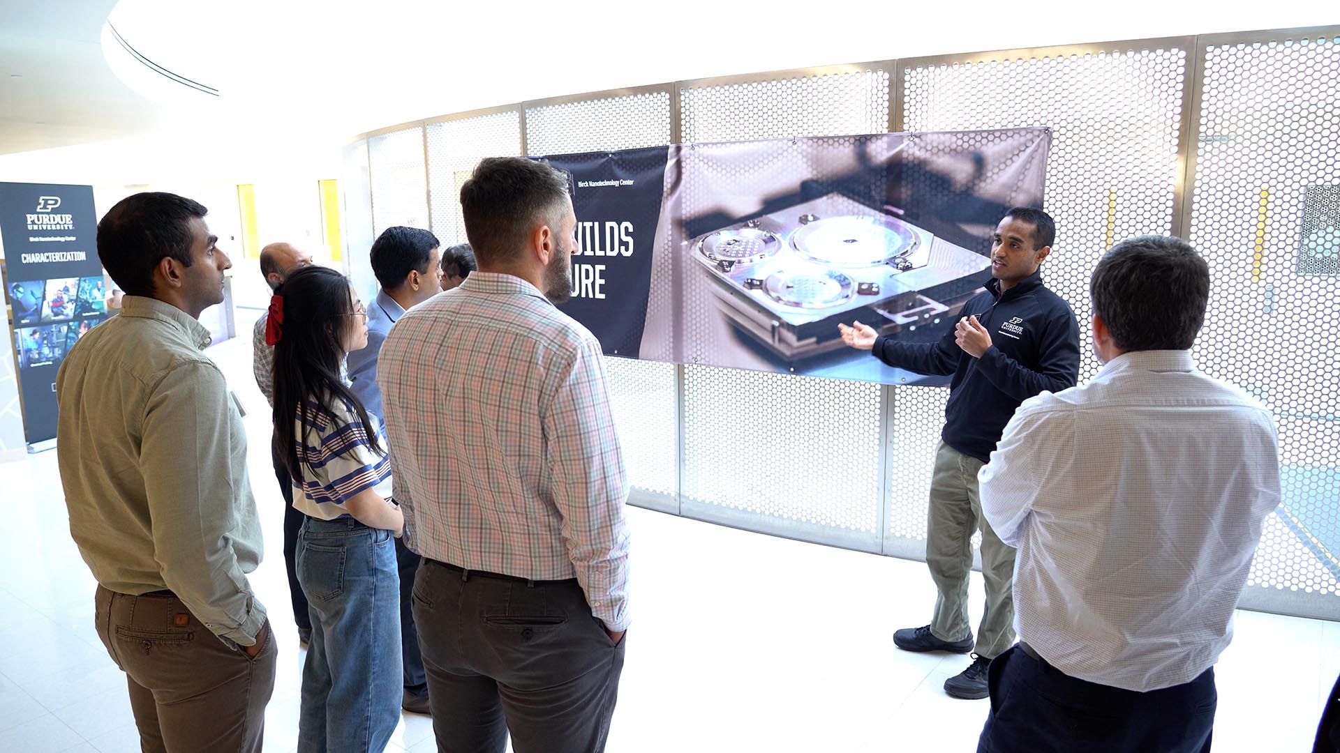
The 125+ attendees also had the chance to see Purdue’s world-class research in person. Students presented information on their respective research projects, and led tours of Purdue’s semiconductor-focused labs and research facilities. One highlight was the Birck Nanotechnology Center, which features one of the largest and highest-grade cleanrooms in all of academia, used for semiconductor fabrication and characterization.
“When it comes to academic research, Purdue is clearly leading the way in advanced packaging,” Subbarayan said. “Now we’re leveraging that research-based expertise with the manufacturing expertise of the world’s leading semiconductor industry partners. Together we will work on substantive projects that move the field forward and create real-world innovations for products and users all around the world.”
Source: Ganesh Subbarayan, ganeshs@purdue.edu
- Event site that has details about the speakers: https://engineering.purdue.edu/Engr/AboutUs/News/Events/2026/international-advanced-system-integration-and-packaging-workshop
-
ASIP website: https://engineering.purdue.edu/ASIP