
ASIP Consortium Kickoff Workshop - October 6-7, 2026
October 6-7, 2026
ASIP invites you to attend the kickoff workshop on October 6-7, 2026. Please RSVP to Ganesh Subbarayan (ganeshs@purdue.edu) with copy to Betsy Baxter (ebaxter@purdue.edu).
As transistor scaling according to Moores law slows, future applications will require novel system integration solutions to achieve performance, power, and cost tradeoffs while ensuring efficient power conversion and delivery, signal and power integrity, sustainability, testability, and security goals. Increasingly, future electronic systems for computing, mobile communications, IoT, automotive, defense and biological applications will rely on advanced integration of separately manufactured chiplets into a 2.5D/3D System-in-Package (SiP).
This consortium kickoff workshop will bring together industry and academic leaders to address research, lab-to-fab translation, and partnership needs in advanced packaging. Sessions include keynotes from SK hynix and AMD, technology highlights from GlobalFoundries, Lam Research, imec, and Dassault Systèmes, panels on materials, reliability, metrology, and academic research needs, Purdue faculty research overviews, and lab tours.
Highlights
- Keynote talks by SK hynix and AMD
- Four technology highlight talks by industry experts from GlobalFoundries, Lam Research, imec, and Dassault Systèmes
- Two panel discussions, one by leading industry experts on materials, reliability and metrology, and the second by leading academic researchers
- Purdue faculty research overviews and lab tours
- Student poster session and reception
- Tours of Birck Nanotechnology Center, Flex Labs, CTRC, and CoSMAP labs
Recent News
- Purdue-led $4.05 million award involving nine PIs from five universities (Purdue, Binghamton University, Penn State University, UCLA, and University of Minnesota) under the SRC SPARC track INSPIRE: INnovation in System Packaging and Integration REsearch was announced on August 18, 2026. Read the announcement.
- On August 27, 2026, SK hynix officially broke ground for its HBM production base in West Lafayette, Indiana. As part of the ceremonies, Purdue signed an MOU for Advanced Packaging R&D with SK hynix. More information.
Agenda
Location: East/West Faculty Lounges (Rooms 240 and 250), Purdue Memorial Union, Purdue University, West Lafayette, IN 47907
October 6, Tuesday " Open session
|
7:30-8:30 AM |
Registration and breakfast |
|
8:30-8:45 AM |
Welcome remarks by Purdue administration |
|
8:45-9:00 AM |
ASIP Overview |
|
9:00-9:45 AM |
Keynote 1: Dr. Hoyoung Son (SK hynix) Advanced Packaging Technology and Future R&D Opportunities in West Lafayette |
|
9:45-10:15 AM |
Keynote 2: Dr. Raja Swaminathan (AMD) Future of AI Hardware Enabled by Advanced Packaging |
|
10:15-10:30 AM |
Coffee Break |
|
10:30-10:50 AM |
Technology Highlights 1: Mr. Scott Pozder (GlobalFoundries) Reliability Challenges and Qualification Strategy for Co-Packaged Optics (CPO) |
|
10:50 AM-12:00 PM |
Purdue faculty research highlights |
|
12:00-1:00 PM |
Lunch and Group Photo |
|
1:00-1:20 PM |
Technology Highlights 2: Dr. Prahalad Parthangal (Lam Research) Advanced Packaging Equipment-Materials Co-Optimization and Challenges |
|
1:20-1:40 PM |
Technology Highlights 3: Dr. Jonathan Prange (imec) Advanced Packaging Programs and Purdue Partnership |
|
1:40-2:45 PM |
Panel Discussion 1 Materials, Reliability, and Inspection challenges |
|
2:45-3:00 PM |
Coffee Break |
|
3:00-3:20 PM |
Technology Highlights 4: Mr. John Maculley (Dassault Systèmes) From Lab to Fab: Building the Future of Advanced System Integration |
|
3:20-4:00 PM |
Panel Discussion 2 Academic Research Needs and Funding Challenges |
|
4:00-6:30 PM |
Tours Birck Nanotechnology Center, Flex Labs, CTRC, and CoSMAP labs |
|
6:30-7:00 PM |
Reception and 30-second student introductions to their posters |
|
7:00-8:30 PM |
Dinner + student posters |
October 7, Wednesday " Closed session for current ASIP consortium members
|
8:30-9:00 AM |
Breakfast |
|
9:00-10:30 AM |
Industry needs discussion |
|
10:30-10:45 AM |
Coffee Break |
|
10:45 AM-12:00 PM |
Discussion and prioritization of project topics |
|
12:00 PM |
Box lunch and adjourn |
Keynotes and Technology Highlights
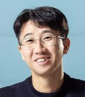 |
Dr. Hoyoung Son
Vice President and Head of Advanced Packaging Development Advanced Packaging Technology and Future R&D Opportunities in West Lafayette Hoyoung Son serves as Vice President and Head of Advanced Package Development at SK hynix, where he has dedicated over 18 years to advanced packaging technologies. Holding a Ph.D. in Material Science and Engineering from KAIST, he currently leverages his expertise in advanced packaging to lead the companys strategic initiatives to evolve into a total AI-memory provider. Dr. Son has been instrumental in establishing SK hynixs global leadership in AI memory, particularly through the development of High Bandwidth Memory (HBM). He spearheaded the package development for SK hynixs first HBM product, overseeing the early introduction and implementation of Through-Silicon Via (TSV) technology, the core foundation of HBM. Furthermore, he led the development of the companys proprietary Mass Reflow-Molded Underfill (MR-MUF) technology. His expertise spans 3D/TSV stacking, 2.5D System-in Package (SiP), and wafer-level packaging. Today, he continues to drive advanced packaging innovations to strengthen SK hynixs technological dominance in the AI era. |
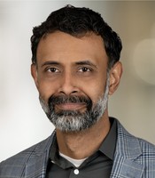 |
Dr. Raja Swaminathan
Corporate Vice President of Heterogeneous Integration Technologies Future of AI Hardware Enabled by Advanced Packaging Dr. Raja Swaminathan is the Corporate Vice President of Heterogeneous Integration Technologies at AMD, spearheading the development of AMD's advanced packaging and heterogeneous integration roadmap. He also leads the Optics technology development at AMD, driving innovation in high-speed optical interconnects and photonics integration. With a distinguished career spanning roles at Intel, Apple, and now AMD, Dr. Swaminathan's expertise in design-technology co-optimization and dedication to optimizing power, performance, area, and cost (PPAC) have led to significant technological advancements such as EMIB, Apple's Mx packages, 3D V-Cache, and 3.5D architectures for AI accelerators. Dr. Swaminathan holds a PhD from Carnegie Mellon University and an undergraduate degree from IIT Madras. With over 100 patents and more than 40 published papers to his name, he was recently recognized as an IEEE Fellow and serves as a technical advisor to multiple startups. His unwavering commitment to heterogeneous integration continues to drive the boundaries of silicon technology. He also shares his insights on life and leadership, drawing lessons from the semiconductor industry, on his LinkedIn profile. |
 |
Mr. Scott Pozder
Senior Member of Technical Staff in Reliability Engineering Reliability Challenges and Qualification Strategy for Co-Packaged Optics (CPO) Scott Pozder is a Senior Member of Technical Staff in Reliability Engineering at GlobalFoundries in Malta, New York. He specializes in semiconductor reliability, statistical analysis, qualification testing, and failure analysis. Scott works with cross-functional teams to improve product robustness and manufacturing reliability across advanced semiconductor technologies. He is an inventor of more than 20 Issued U.S. Patents in the areas of 3D IC, Advanced Packaging and Cu BEOL. |
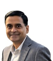 |
Dr. Prahalad Parthangal
Technical Director of Advanced Packaging Advanced Packaging Equipment-Materials Co-Optimization and Challenges Prahalad Parthangal is a Technical Director of Advanced Packaging at Lam Research based in Tualatin, OR. He is responsible for customer engagements and enabling heterogeneous integration roadmaps for all North American customers of Lam. He also leads strategic programs with research institutions, consortia, and universities on emerging packaging technologies. Prior to joining Lam in 2025, he was a Principal Engineer at Intel Corporation with over 17 years of experience in process technology development across leading edge logic foundry nodes, die prep assembly, and strategic equipment technology sourcing. He has led early evaluations and qualifications of several breakthrough-equipment and process technologies throughout his career, from pathfinding through development and HVM phases. He received his MS degree from the University of Minnesota, Twin Cities and his PhD from the University of Maryland, College Park |
 |
Dr. Jonathan Prange
Technical Program Director and Portfolio Manager Advanced Packaging Programs and Purdue Partnership Jonathan is a Technical Program Director and Portfolio Manager at IMEC. In this role, he is responsible for building and maintaining a project portfolio for advanced packaging, focusing on platform development to enable advanced integration through hybrid bonding, fine-line RDL and 2.5D Si interposer interconnect architectures. As a leader within the US Operations team, he also supports the collaborations and technical projects being executed in support of BE-based programs. Before joining IMEC, Jonathan was at MITRE working on semiconductor strategy and business development. Prior to MITRE, he spent over 10 years at first Dow, which later became DuPont Electronic Materials, focusing on developing new metallization and dielectric materials for advanced packaging applications with increasing levels of responsibility and leadership. Jonathan holds a B.S. from Purdue University and a PhD from Stanford University. |
 |
Mr. John Maculley
Director of Global High-Tech Industry Business Consulting From Lab to Fab: Building the Future of Advanced System Integration John Maculley is Director of Global High-Tech Industry Business Consulting at Dassault Systèmes, where he leads global business strategy across semiconductors, electronics, AI infrastructure, advanced packaging, and industrial engineering. He connects customers, technology partners, and academic ecosystems to develop scalable, practical applications of virtual twins, multiphysics simulation, model-based systems engineering, AI-Physics, and agentic engineering. His work includes strategic initiatives with NVIDIA focused on silicon-to-AI-factory engineering, model-based reference architectures, accelerated simulation, extreme co-design, and AI agents that orchestrate engineering knowledge and tools. He also leads Dassault Systèmes engagement with Purdue University on advanced system integration, Lab-to-Fab innovation, and workforce development. Previously, John advised C-suite leaders at semiconductor companies, spent 12 years at Micron Technology leading process R&D and operational excellence, and supported aerospace programs at NASA. He also taught graduate business courses at Boise State University. John holds an MBA from William & Mary and a BS from San Diego State University. |
Panel Discussion 1: Materials, Reliability, and Inspection Challenges
October 6, 2026, 1:40-2:45 PM
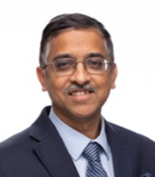 |
Dr. Venky Sundaram
Founder and President Dr. Venky Sundaram is Founder and President of 3D System Scaling LLC, focusing on C-Suite advisory, innovation management, business development, technology roadmaps, partner ecosystem development, and new business creation. Dr. Sundaram holds a BS from the Indian Institute of Technology, Bombay, M.S. and Ph.D. from the Georgia Institute of Technology, Atlanta, GA. Venky is a globally recognized leader and entrepreneur in heterogeneous integration and advanced semiconductor packaging with over 25 years of experience in commercializing new technologies. |
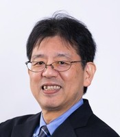 |
Dr. Yutaka Uematsu
Principal Researcher Yutaka Uematsu, Ph.D., is a Principal Researcher at Hitachi, Ltd., where he leads research on advanced semiconductor packaging, chiplet integration, and reliability. Since joining Hitachi in 2001, he has worked on signal and power integrity, high-speed interfaces, and the design and evaluation of advanced electronic systems. His current research focuses on multiphysics modeling and AI-assisted design for 2.5D/3D integration, as well as advanced design and evaluation technologies for semiconductor packaging and the advancement of inspection systems for advanced back-end semiconductor manufacturing. He is also a Visiting Researcher at the National Institute of Advanced Industrial Science and Technology (AIST), where he conducts research on chiplet package design. He received his Ph.D. from Tohoku University in 2001 and is a Senior Member of both IEEE and the Institute of Electronics, Information and Communication Engineers (IEICE). |
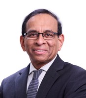 |
Dr. Devan Iyer
Chief Strategist for Advanced Electronic Packaging Dr. Devan Iyer is the Chief Strategist for Advanced Electronic Packaging at Global Electronics Association since March 2024. Devan has more than 35 years of leadership experience in Advanced electronic packaging at component and module design & technology development, manufacturing and in managing business units. He has served as Senior Vice President in Amkor Technology and Corporate Vice President at Texas Instruments in Technology & Manufacturing Group. He has also worked for Infineon Technologies & General Electric. As R&D Director he has also led several industry consortia in electronic packaging at Institute of Microelectronics in Singapore and at the Packaging Research Center at Georgia Tech in Atlanta. Devan has 35 patents to his credit and holds advisory board positions in several companies in Advanced packaging supply chain. |
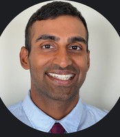 |
Mr. Vinayak Kedlaya
Packaging R&D Engineer Vinayak graduated from BMS college of engineering with a bachelors in mechanical engineering in 2014 and from Carnegie Mellon University with a Masters in mechanical engineering in 2017. His graduate research focused on in-operando X-ray computed tomography in electrochemical systems. He began his career at Intel in early 2017 as a Packaging R&D Engineer working on developing the singulation process. In 2019 he went on to work on the substrate die embedding and backend processes for the 1st generation EMIB product (Sapphire Rapids). In 2022 he was the pathfinding lead for developing key building blocks to enable 224G SerDes capabilities. Most recently his work has been focused on driving Intels Co-packaged Optics roadmap. In his spare time he enjoys playing tennis, swimming and spending time with his wife and two dogs. |
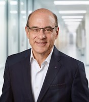 |
Dr. Charles Woychik
Vice President of Business Development Charles Woychik is currently the VP of Business Development at NHanced Semiconductors, Inc. Previously he was Senior Director of Advanced Packaging Platforms at SkyWater Technology. Chuck has held technical and managerial positions at i3 Microsystems, Invensas, GE Global Research, and IBM. He holds a Doctorate and Masters of Science degree in Materials Science and Engineering from Carnegie-Mellon University. He has a Bachelors of Science degree in Materials Science from the University of Wisconsin, Madison. Chuck has numerous publications and 123 issued US patents to his credit. |
Panel Discussion 2: Academic Research Needs and Funding Challenges
October 6, 2026, 3:20-4:00 PM
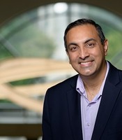 |
Prof. Nikhilesh Chawla
Associate Dean for Research and Innovation in the College of Engineering and Ransburg Professor in the School of Materials Engineering Nikhilesh Chawla is the Associate Dean for Research and Innovation in the College of Engineering at Purdue University and Ransburg Professor in the School of Materials Engineering at Purdue University. He joined Purdue in 2020, after previously serving as Founding Director of the Center for 4D Materials Science and Fulton Professor of Materials Science and Engineering at Arizona State University. Prof. Chawla received his Ph.D. in Materials Science and Engineering from the University of Michigan in 1997. He has served as the inaugural Associate Dean for Engineering in Indianapolis, Acting Head of the School of Materials Engineering, and Co-Director of the Semiconductor Degree Programs at Purdue. Prof. Chawlas research is in the area Four-Dimensional (4D) materials science with a particular emphasis on the deformation behavior of advanced materials at bulk and small length scales. He has co-authored over 320 refereed journal publications (Google Scholar h-index of 71) and over 620 presentations in these areas. He has close to 18,400 citations to his work. He is the author of the textbook Metal Matrix Composites (co-authored with K.K. Chawla), published by Springer. Prof. Chawla is a Fellow of the Minerals, Metals, and Materials Society (TMS) as well as a Fellow of ASM International. He is the recipient of the Innovation in Materials Characterization Award (Materials Research Society, 2024), Hes also won the National Science Foundation Early Career Development Award and the Office of Naval Research Young Investigator Award. Prof. Chawla was an editor for Materials Science and Engineering A published by Elsevier between 2012-2024 (2022 Impact Factor of 6.4). He also serves on the Editorial Boards of Materials Characterization and Materials Chemistry and Physics. |
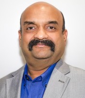 |
Mr. Girish Wable
Technology Program Director Girish Wable is a technology, operations, sourcing, and business solutions strategist with more than 30 years of global experience in electronics manufacturing, high-performance coatings, automation, additive manufacturing, printed electronics, and digital transformation. He specializes in developing and implementing strategic engineering, technology, operational, and business initiatives that drive innovation and growth. Girish has authored numerous technical publications, held multiple patents, and actively engaged with industry partners and research institutions to advance emerging technologies. He regularly contributes to engineering articles, reviews technical proposals for startups and small businesses, serves on advisory boards, and has been a keynote speaker at several conferences. At Semiconductor Research Corporation (SRC), Girish serves as a Technology Program Director, leading the development of collaborative research programs that connect semiconductor companies, universities, and strategic stakeholders. He has been helping conceptualize, shape, launch and program manage initiatives such as SPARC, a project-based pathfinding research program. He continues to work on securing industry participation commitments and negotiating membership agreements. He holds a Bachelor of Science in Mechanical Engineering, a Master of Science in Industrial Engineering, and an MBA focused on innovation and entrepreneurship. Girish has been involved with industry research consortia since 2001, beginning as an intern at Jabil and later participating in the development and operation of multiple consortium initiatives as an industry Representative. |
 |
Prof. Bahgat Sammakia
Distinguished Professor of Mechanical Engineering Professor Bahgat G. Sammakia is a Distinguished Professor of Mechanical Engineering at Binghamton University and a widely recognized leader in thermal management, electronics packaging, and heat transfer. He has built a distinguished career spanning both academia and industry, including senior technical leadership roles at IBM and major academic leadership positions at Binghamton University, where he served as Vice President for Research from 2011 to 2025. He is also the founding director S3IP,a NY State Center of Excellence, and ES2 an NSF IUCRC center. This reflects his long-standing commitment to advancing innovation in electronic systems, heterogeneous integration, and energy-efficient technologies. Over the course of his career, Professor Sammakia has authored more than 350 peer-reviewed publications, earned over 11,000 citations, and developed a substantial patent portfolio in advanced cooling, packaging, and thermal-management technologies. His work has had a broad impact on next-generation electronic systems and data center efficiency, and he has been recognized with numerous honors, including election as Fellow of the ASME, and the IEEE. He has received the ASME Heat Transfer Memorial Award, and Fellow status in the National Academy of Inventors. |
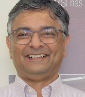 |
Prof. Sachin Sapatnekar
Distinguished McKnight University Professor and Robert and Marjorie Henle Chair Sachin Sapatnekar received the B. Tech. degree from the Indian Institute of Technology, Bombay, the M.S. degree from Syracuse University, and the Ph.D. degree from the University of Illinois. He is currently on the faculty of the University of Minnesota, where he holds a Distinguished McKnight University Professorship and the Robert and Marjorie Henle Chair. His research interests include heterogeneous integration,EDA for analog and digital systems, and emerging computing paradigms and technologies. He has published widely on these topics and been the General Chair and Technical Program Chair for the Design Automation Conference (DAC) and Editor-in-Chief of the IEEE Transactions on Computer-Aided Design of Integrated Circuits and Systems (TCAD). In addition to several Best Paper awards, he has received the SRC Technical Excellence Award, the SIA University Research Award, and the ACM SIGDA Pioneering Achievement Award. He is a Fellow of the ACM and the IEEE. |
 |
Prof. José Schutt-Ainé
Professor of Electrical and Computer Engineering José Schutt-Ainé is with the faculty in the Electrical and Computer Engineering Department at the University of Illinois at Urbana-Champaign. His research interests are on signal integrity for high-speed digital and high-frequency applications. Dr. Schutt-Ain is an IEEE Life Fellow, EPS Distinguished Lecturer, and served as Co-Editor-in-Chief of the IEEE Transactions on Components, Packaging and Manufacturing Technology (T-CPMT) from 2007 to 2018. He is currently chairing the Co-design chapter of the IEEE-EPS Co-Design Chapter of the Heterogeneous Integration Roadmap. He received the 2024 IEEE-EPS Outstanding Sustained Technical Contribution Award. |
About Microelectronics Research and Education at Purdue University:
College of Engineering at Purdue University is ranked 4th in the US and graduates more engineers than the top three ranked institutions combined. Purdues excellence at scale is exemplified by the many national and international microelectronic research centers at Purdue that have received over $250 million in research funding. Specifically, in Advanced System Integration and Packaging, Purdue hosts five centers that together conduct nearly $90 million in research. Purdue University, through its expert faculty, is actively involved in guiding the formulation of the CHIPS Act R&D programs and is vigorously engaged with industry partners on all elements of CHIPS Act programs.
Complementary to the research mission, Purdue created the nations first MS degree program in semiconductors, with more than 55 Purdue faculty members teaching over 100 courses on semiconductors and advanced packaging. Purdues educational innovations to motivate talented undergraduate students to pursue careers in semiconductors include the freshmen-level seminar course Changing the World with Chips - Introduction to Semiconductors, and a unique eight-week hands-on experience in chip design and fabrication termed Summer Training, Awareness, and Readiness for Semiconductors (STARS). More information at https://engineering.purdue.edu/semiconductors.
Contact: Betsy Baxter or Ganesh Subbarayan