Purdue Engineering faculty spearhead semiconductor ecosystem
Semiconductors have emerged as the heartbeat of technology, powering everything from smart phones and transportation to GPS navigation, weather prediction, energy, healthcare, defense, digital agriculture and the compute heft underpinning the most advanced AI learning and inference data centers on Earth.
For decades, the U.S. steadily outsourced much of its semiconductor manufacturing. While that improved efficiency and reduced costs in the short term, it created major vulnerabilities. The pandemic made those risks visible to everyone, but for the defense and advanced technology communities, this has been a known concern for a long time. A reliable onshore supply chain is no longer optional—it is a strategic necessity.
Led by Mark Lundstrom, special advisor to Purdue University President Mung Chiang and the Don and Carol Scifres Distinguished Professor in the Elmore Family School of Electrical and Computer Engineering (ECE), a team of faculty works closely with Chiang to bring Purdue’s long-standing strengths in semiconductors to support the nation’s response to its semiconductor challenges.
“A university that aims to be the most consequential university in the nation should address the most consequential problem that the country currently faces, and that is the semiconductor challenge, because it is the foundation to our nation’s security and economic prosperity” Lundstrom said. “The fact that we, as the largest STEM universities in the country, have made this a university priority is a reflection of the responsibility we feel to help the nation address this challenge. That’s what a consequential university does.”
The drive to make Purdue “The Semiconductor University” is a wide-ranging team effort. It begins with talent development. The Semiconductor Degrees Program, directed by professor David Janes, is an ambitious program to develop talent for the commercial sector of the semiconductor industry. Scalable Asymmetric Lifecycle Engagement (SCALE), directed by Peter Bermel, Elmore Professor of ECE, and Kerrie Douglas, associate professor in the School of Engineering Education, is the nation’s premier workforce development program for the defense sector.
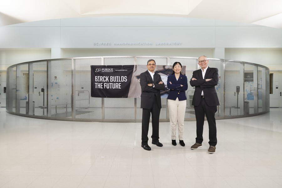
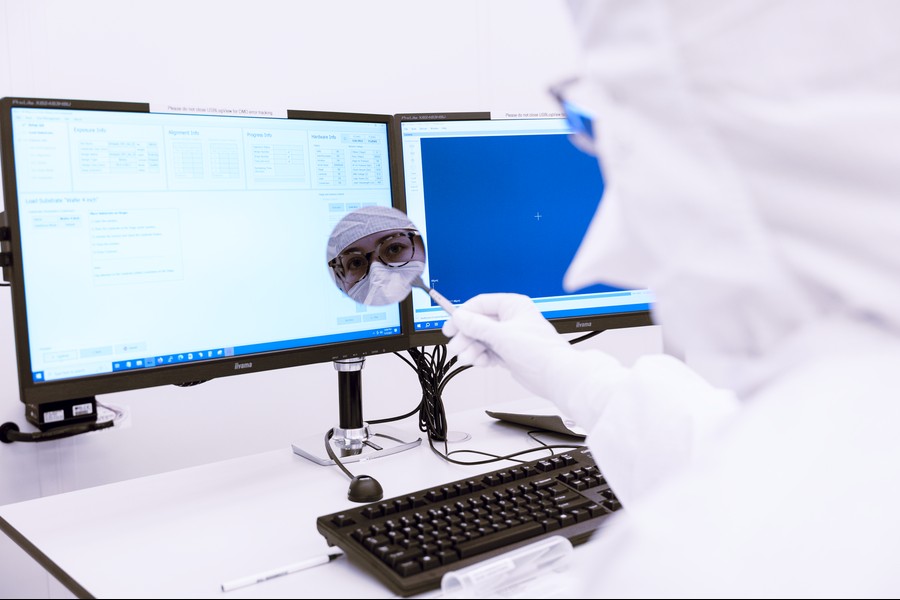
Four major translational research centers and institutes work in partnership with companies to bring the fruits of university research to the marketplace. The Atalla Institute for Advanced System Integration and Packaging (ASIP) focuses on the advanced packaging and heterogeneous integration – the so-called fourth wave of semiconductor technology. ASIP director Ganesh Subbarayan, the James G. Dwyer Professor in the School of Mechanical Engineering, leads a team of 35 faculty. The Birck Nanotechnology Center, the nation’s finest academic semiconductor research facility, is directed by Zhihong Chen, the Reilly Professor of ECE and the Mary Jo and Robert L. Kirk Director of Birck, which supports more than 600 users annually, including external users. The Center for Secure Microelectronic Ecosystems (CSME) is a unique academic, industry, and government partnership with a mandate to address the challenges of secure microelectronics. CSME is co-directed by Joerg Appenzeller, the Barry M. and Patricia L. Epstein Professor of ECE, and Anand Raghunathan, the Silicon Valley Professor of ECE. Finally, the Institute for Chips and AI is co-directed by Raghunathan and Kaushik Roy, the Edward G. Tiedemann Jr. Distinguished Professor of ECE.
Supporting these major workforce development and research and innovation programs is nanoHUB and its Chipshub, which are co-directed by Gerhard Klimeck, Elmore Professor of ECE and Alejandro Strachan, the Reilly Professor in the School of Materials Engineering. nanoHUB and Chipshub provide online access to simulations, data and educational resources, which provide Purdue with global impact.
Purdue’s semiconductor team is spearheading a drive to make Purdue central — as an educational, research and workforce development powerhouse — to American independence and supremacy in semiconductor design, manufacture, testing and skilled talent.
The stakes couldn’t be higher.
From model rockets to 3-nanometer chips
Mark Lundstrom’s fascination with technology started early, in a small town in rural Minnesota. “I was always shooting off model rockets, putting together a shortwave radio kit, building my own telescope, ham radio, etc.,” he said. “It seems that I was meant to be an engineer.”
He found plenty — of engineers and role models — in college. He got his bachelor’s and master’s degrees in electrical engineering at the University of Minnesota and his PhD in that field at Purdue.
“What really piqued my interest was a course on integrated circuit engineering that I took as a junior,” he said. “It was taught by a real semiconductor pioneer who had retired from industry just two years before; he told us, ‘I’ve been out of the industry for two years, and I am completely out of date.’ Things move fast in the semiconductor industry — that sounded exciting to me. I began to learn how deep, interesting and important semiconductor science is.”
After his master’s, he worked in the private sector, joining Hewlett-Packard (HP) to develop an integrated circuit manufacturing process to produce chips for HP desktop computers. It was a 5-micron process at the time. “State-of-the-art today is 3 nanometers — the area of a modern transistor is more than 1,000,000 times smaller than the transistors we were making,” he said. “Even so, it was really hard then to make the manufacturing work.”
Lundstrom began as a PhD student at Purdue working on solar cells. At the time, he had no intention of becoming a professor. “After receiving my doctorate, I decided to try being a professor for a few years. That has now turned into 45 years on the Purdue faculty.”
At Purdue, he’s worked on semiconductor devices, solar cells, transistors, semiconductor lasers and thermoelectric devices. Most of this work was in theory, modeling and computer simulation. The research that had the most impact? “How small can a transistor be?”
One by-product was nanoHUB, the world’s largest science gateway for nanoelectronics. On nanoHUB, users can run sophisticated computer simulations of semiconductor materials and devices and can view open-content educational resources. “Now under the leadership of my colleagues, Gerhard Klimeck and Alejandro Strachan, nanoHUB is 30 years old and going strong,” Lundstrom said.
He said it’s hard to overstate the importance of semiconductor technology. He thinks Isaac Asimov may have come closest when he called the invention of the silicon chip “the most important moment since mankind emerged as a life form.”
The key elements of Semiconductors@Purdue are talent development, research to accelerate innovation, and economic development — bringing the semiconductor industry to the nation’s heartland and the Greater Lafayette region.
Education is paramount. “We have two of the nation’s most ambitious workforce development programs at Purdue,” according to Lundstrom. “The Semiconductor Degrees Program addresses the commercial sector and is advised by a 40-member leadership board of senior semiconductor executives and led by my colleague, Professor David Janes. SCALE is a 35-university network led by my Purdue colleagues, Peter Bermel and Kerrie Douglas, and is the preeminent U.S. program for semiconductor workforce development in the defense sector.”
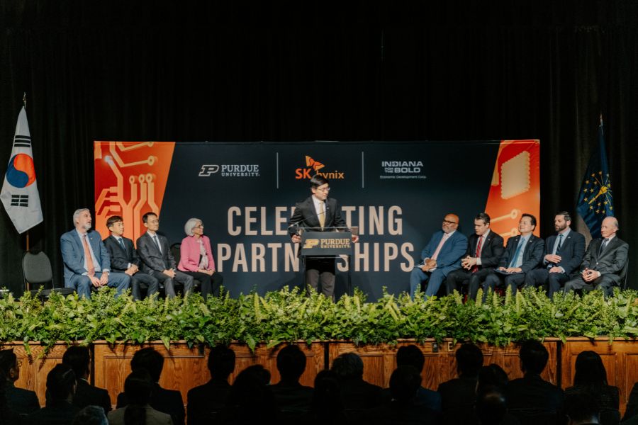
Purdue’s efforts in semiconductors are bearing fruit. Over the past three years, three global semiconductor leaders have elected to locate in West Lafayette near and even on the Purdue campus. MediaTek, the fifth largest chip design company in the world, opened its first Midwest office on Purdue’s West Lafayette campus in 2025. In 2024, SK hynix, the global leader in memory chips for AI, announced its plans for an advanced packaging manufacturing facility and research and development lab near the Purdue campus. Imec, the world’s largest independent semiconductor R&D organization, launched a research partnership at Purdue in 2023.
“The stage is set for even bigger opportunities,” said Lundstrom. “The U.S. is investing in leading-edge semiconductor manufacturing in only seven regions of the country. These clusters were established 30, 40, even 50 years ago and continue to grow. West Lafayette is poised to become the nation’s newest, the first leading-edge semiconductor cluster in the heartland.”
Lundstrom is a life fellow of the Institute of Electrical and Electronic Engineers (IEEE), the American Physical Society, and the American Association for the Advancement of Science. He has received several awards for his teaching, research, and outreach, and is a member of the U.S. National Academy of Engineering and the American Academy of Arts and Sciences.
In 2024, then-Indiana Gov. Eric Holcomb named him a “Sagamore of the Wabash” for his contributions to semiconductors in Indiana. The word “sagamore” was used by the tribes of the northeastern U.S. to describe a great man among the tribe to whom the chief would look for wisdom and advice. It is a personal tribute for those who have rendered distinguished service to Indiana and have contributed greatly to the Hoosier heritage.
Lundstrom initially led Chiang’s task force of semiconductor faculty. As the initiative matured, a Semiconductor Leadership Council reporting to the dean of the College of Engineering was established. Lundstrom is now stepping back from day-to-day operations and taking on a more strategic role. The long-term success of the semiconductor ecosystem that is beginning to emerge around Purdue continues to be his highest priority, but “as soon as I can find the time, there is also a research problem that I would like to tackle and the third edition of my textbook to complete,” he added.
And after hours? “I unwind by trying to get my 10,000 steps in every day, reading, hiking and being on my motorcycle every chance I get.”
Bridging physics and engineering at the nanoscale
Zhihong Chen works with Lundstrom as chair of the Semiconductor Leadership Council. “The strength of Purdue’s semiconductor ecosystem really comes from teamwork,” she said. She works with a focused group of faculty spanning the full semiconductor “innovation stack.” Appenzeller brings internationally recognized leadership in advanced device research, while Roy and Raghunathan contribute deep expertise in circuits and system design. Bermel initiated Purdue’s semiconductor workforce development efforts through the SCALE program; Professor Vijay Raghunathan spearheads Purdue’s global semiconductor programs; and Subbarayan adds critical capabilities in mechanical and thermal modeling and advanced packaging. As the effort grew, more colleagues, including Muhammad Alam, John Howarter, Janes, Dan Jiao, Strachan and others joined and expanded the team’s reach. Together, these complementary strengths position Purdue to address semiconductor challenges from materials and devices to systems, packaging, and workforce development.
Chen focuses on building the research infrastructure and translational ecosystem through the Birck Nanotechnology Center — expanding fabrication and characterization capabilities, integrating digital twins and AI into semiconductor R&D, and creating standardized platforms such as test vehicles that accelerate lab-to-fab transition. “Together, the team represents different but highly complementary parts of the semiconductor stack.”
Like Lundstrom, her scientific interests were piqued early. “It began with physics in high school,” she recalled. “I felt truly fascinated by science. What captured me was not just learning formulas but realizing that physics could explain the world in a logical, coherent way. Suddenly, everyday phenomena such as motion, light and electricity were no longer mysterious. They all made sense. That sense of clarity and structure was incredibly powerful to me.”
She originally trained in physics, getting a rigorous foundation in fundamental science. Her interest in semiconductors emerged during her PhD studies at the University of Florida, when nanomaterials and nanotechnology were becoming experimentally accessible. “At that time, new tools and equipment were finally allowing scientists to explore matter at the nanoscale in a serious way. It felt like the door to a completely new world had just opened.”
Like Lundstrom, Chen benefited greatly from practical experience in the private sector.
“My time at the IBM T. J. Watson Research Center was truly formative for my career. IBM shaped my passion for bridging the gap between discovery and application. We were not only asking ‘Can this new material work?’ but also ‘Can it scale? Can it be manufactured? Can it be integrated into real semiconductor technology?’ That mindset shaped how I think about research. When I moved into academia, I carried that philosophy with me: pushing fundamental science forward, but always with a vision for how it can transition into real technology.”
Chen joined Purdue in 2010, focusing on low-dimensional semiconductors and exploring new transport phenomena and novel logic concepts. Over time, she expanded her research to interconnects and memory. She explored non-conventional computing schemes, including spintronics and other non-von Neumann computing concepts such as probabilistic computing.
“A major milestone in my career at Purdue was serving as the director of the Semiconductor Research Corporation (SRC) nCORE NEW LIMITS Center, a large multi-university, industry-sponsored research center focused on advancing 2D materials for logic, memory and interconnect technologies,” she said. “That experience deeply strengthened my role in leading large, collaborative, industry-facing research programs.”
Chen served as associate director of research at Birck from 2019 to 2021, interim director in 2022, and now as director. She oversees one of the most advanced academic nanofabrication and characterization facilities in the country and leads its expansion into translational semiconductor R&D, quantum research, and AI-driven and digital-twin-enabled innovation.
“There is a critical gap in the lab-to-fab transition in the United States,” she said. “We remain the world leader in fundamental research and innovation, but too many breakthroughs stall before they reach manufacturable technology. We hope Birck can become a national facility that provides a platform for innovators to transfer their ideas to market. Purdue’s role is not to replace industry — it is to reduce the cost and time for innovation, accelerate lab-to-fab transition and create a workforce that makes the entire system work.”
Her work is focused on lab-to-fab acceleration, industry-relevant test vehicles, digital twins for semiconductor fabrication and processing, and experiential workforce development. She helped launch hands-on education training programs such as Semiconductors@Birck and Virtual Twins@Birck, which connect students to actual fabrication, characterization and digital manufacturing workflows.
She and her collaborators are using AI and machine learning to search complex materials and process spaces, design experiments, learn from real data and rapidly converge on new fabrication methods that would be impossible to find otherwise. “I am particularly excited about autonomous,” she said. “I see this as a powerful way to accelerate materials and process innovation in the coming decade.”
Chen feels most proud of having helped build bridges — between physics and engineering, between academia and industry, and between early discovery and real-world impact. “From my time at IBM to my years at Purdue, I have tried to work at that interface, where fundamental ideas are tested against real technology development needs.”
She’s also made her mark as an educator. “Seeing students go on to lead in industry, startups, national labs and academia is, for me, the most meaningful measure of success,” she said. “If I were to think about legacy, I would like it to be this: that I helped create platforms and communities that outlast any single project — research platforms, training pipelines and collaborations that continue to enable innovation long after I step aside.”
Chen has been highly awarded for her work. She is an IEEE Fellow, recipient of the Intel Rising Star Faculty Award, the Ruth and Joel Spira Excellence in Teaching Award and the Purdue University Excellence in Research Award. She was a university Faculty Scholar from 2017-2022.
Personal recognition aside, though, her overarching mission, through her collaboration with all semiconductor colleagues, focuses on the larger picture — fashioning the Purdue microelectronics and nanotechnology ecosystem into “The Semiconductor University.”
“Our collective goal is to make Purdue not just a place where semiconductor research happens, but a place where industry, government and academia converge to solve national challenges — whether that is rebuilding domestic manufacturing, training the next generation workforce or accelerating innovation from discovery to market.”
Packaging it all together
Like Lundstrom and Chen, Ganesh Subbarayan’s deep industry experience helped shape and inform his research. In his case, he worked for IBM in an electronics packaging development lab in Endicott, New York. “I chose to join IBM since I found the opportunity to solve ‘real’ engineering problems interesting,” he recalled.
The lab was filled with leaders of the electronics packaging field. His department had the largest number of mechanical engineers in the company, and its role was to solve thermomechanical challenges that arose during electronics packaging development. “I greatly enjoyed the ‘forensic’ nature of the mechanical failure problems I was asked to solve,” he said. “I am very grateful for the IBM experience, which is the foundation of my academic research career.”
His expertise in computational science is useful to today’s modeling of semiconductor packages. Historically, electronics packaging was viewed as less critical than chip fabrication, almost an afterthought. But the cost challenge of integrating transistors on ever larger sized chips has forced the industry to seek equivalent function by integrating smaller “chiplets” very close to each other so they function essentially as one large chip.
“This so-called ‘advanced’ packaging — integrating multiple chiplets in very close proximity on advanced substrates — is now a critical factor to achieving the performance, power and size goals of electronics systems at an acceptable cost,” Subbarayan said.
Unfortunately, this semiconductor packaging work was offshored to Asia, beginning in the mid 1990s. “The talent and capability for advanced packaging is not readily available in the United States,” he said. “A White House report published in 2021 stated that only 3% of the global capability for advanced packaging was located here. As the defense industry in particular faces challenges in finding reliable suppliers of components and companies capable of building low-volume systems — indeed, as the entire industry faces talent and capability challenges — reshoring packaging is a critical and immediate need for national security.”
Subbarayan joined Purdue in October 2002. The search committee at the time was particularly interested in someone with a background in mechanical design and the ability to combine computational science with applications in electronics packaging — essentially, someone who combines mechanical curiosity with deep electronics and computational knowledge.
“I had explored more efficient mathematical representations, including mathematical functions from the field of geometrical modeling and artificial neural networks (now referred to as machine learning),” Subbarayan said. “For example, one of the early problems I focused on was how to model the shapes of solder droplets during electronics chip assembly to circuit boards and the variabilities in product life because of uncertainty in the manufacturing process.”
Subbarayan has been continuously funded by SRC and its members over his career at Purdue. His research led to Purdue being awarded the Center for Heterogeneous Integration Research in Packaging (CHIRP) in 2018. He is the co-director of CHIRP, the first SRC center dedicated to advanced packaging. He was also appointed as a founding executive member of a team developing a proposal for the CHIPS Manufacturing USA Institute, which led to the Semiconductor Manufacturing and Advanced Research with Twins (SMART) USA Institute in November 2024.
He emphasizes that microelectronics and advanced packaging are truly multidisciplinary fields. Critical to success is the involvement of electrical designers, fabrication experts who identify new materials, devices and processes, thermal engineers who identify strategies to remove the generated waste heat, and mechanical engineers who assure reliable, manufacturable designs.
“Purdue has perhaps the largest group of faculty researchers in many of these disciplines, and Professor Lundstrom has coordinated this group to work together towards the greater Purdue goal of building a comprehensive semiconductor ecosystem,” Subbarayan said. “His leadership has been critical in setting directions for Purdue. A major outcome of Purdue efforts is SK hynix’s decision to select Purdue as the site for its U.S. memory fabrication facility and advanced packaging R&D line after an intense year of search by the company.”
Subbarayan also heads ASIP, which serves to highlight the Purdue faculty strength in advanced packaging. “The exponential growth in energy consumption in AI computing, advances in the chiplet ecosystem, and the need to trade off speed, power and size with cost, is driving the future of advanced packaging,” he said “ASIP is engaging with anchor partners such as SK hynix, SRC, imec and many others to develop advanced packaging technology quicker and cheaper.”
Like his colleagues Lundstrom and Chen, Subbarayan is the recipient of numerous awards and honors. His research has been recognized with the Mechanics Award by the American Society of Mechanical Engineers (ASME) Electronics and Photonics Packaging Division, ASME fellow election, IEEE fellow election, the SRC Technical Excellence Award, and the IEEE Richard Chu Award for Excellence in Thermal and Thermomechanical Management of Electronics. He has served as Editor-in-Chief of IEEE Transactions on Advanced Packaging, a journal that ranked second-highest by impact factor among all manufacturing journals.
Fitting recognition for a curious, innovative researcher. “I have always enjoyed solving complex ‘real-world’ challenges that underlie manufacturing processes or mechanical failure,” he said. “In academia, I added identifying the failure mechanisms, developing theories governing the phenomena, and numerically modeling the complex physics behind these problems.”
And when he’s not working?
“I enjoy travel with my wife and three kids, visiting museums, and learning about cultures of the world. Long walks with my wife, watching science/nature videos, and computer tech work (my alternative calling) are my ways of relieving stress. I was part of my high school and Indian Institute of Technology Madras cricket teams, and I enjoy watching most sports on TV.”
Purdue Engineering’s semiconductor research is a pillar of Purdue Computes, a strategic university initiative to further scale Purdue’s research and educational excellence in computing.
This story was developed as part of "Victories & Heroes: Your Campaign for Purdue." Join us in elevating Purdue Engineering education and excellence. Click here to be a part of Purdue history.