Purdue Engineering pipeline: Semiconductor Degrees Program builds workforce for critical industry
How Purdue's interdisciplinary approach prepares students for careers across chip design, manufacturing and advanced packaging
Over the next five years, the United States needs at least 50,000 trained semiconductor engineers. It's a staggering number driven by the CHIPS Act's push to return chip manufacturing to American soil and maintain U.S. leadership in chip design. But building fabrication facilities is only half the equation. The real challenge is building the workforce to run them.
"Semiconductors are foundational to everything digital," explains Keyvan Esfarjani, co-chair of Purdue University's Semiconductor Degrees Leadership Board and former Intel executive. "There is not one thing that we do in our lives that doesn't, in one shape or form, have a digital aspect into it. Whether it's your cars, home appliances, computers, data centers and now AI. It's all digital and everything digital is enabled by semiconductors ."
That digital foundation represents a $1 trillion industry spanning across chip design, equipment makers, chemicals, chip fabrication to advanced packaging, assembly and test. Supporting this ecosystem requires talent across multiple disciplines, not just electrical engineering.
"This is a multi-disciplinary profession," Esfarjani emphasizes. "In order to enable this industry, it requires skills across this whole value chain."
Purdue launched its Semiconductor Degrees Program (SDP) in 2022 to help meet this challenge. The program takes a comprehensive approach that prepares students from 25 majors for all sectors of the semiconductor industry.
Building on decades of expertise
The SDP emerged from Purdue's deep expertise in semiconductor research and education. "Purdue's long history in research and education in semiconductors was a key factor in creating SDP and getting company involvement and support," explains David Janes, a professor in the Elmore Family School of Electrical and Computer Engineering who leads the program. "Purdue has had microfabrication facilities for approximately 60 years. The Birck Nanotechnology Center, which is the hub of experimental work in semiconductor materials and devices, celebrated its 20th anniversary in 2025."
What's new is the coordinated, campus-wide scale. "We realized that the broad goals of the CHIPS Act, re-shoring semiconductor manufacturing and maintaining U.S. leadership in chip design, will require a large number of well-trained students," Janes says. "SDP was created to help develop a significant fraction of the talent required by industry."
Students from the College of Engineering, College of Science, the Daniels School of Business and the Purdue Polytechnic Institute participate in the program. It offers a campus-wide semiconductor certificate accessible to all undergraduates, departmental concentrations in four departments, and online master's programs including an interdisciplinary engineering degree.
"'Comprehensive' also refers to addressing the needs of all sectors of the semiconductor industry," Janes explains, "including chip design, manufacturing, equipment, materials and advanced packaging."
Industry partnership shapes curriculum
The Semiconductor Degrees Leadership Board (SDLB) comprises approximately 40 companies whose senior technical leaders meet twice yearly to review programs and provide feedback.
"This collaboration with the industry is super important and the SDLB was designed from the get-go" Esfarjani says. "The university, in collaboration with the industry, is forward thinking about where those future skills are going to be needed so that you can train the students today."
Gregg Bartlett, chief technology officer at GlobalFoundries and an SDLP member, describes the partnership as uniquely effective. “Purdue is extremely well connected. The Semiconductor Degrees Leadership Board has an unprecedented number of industry participants working directly with Purdue and the leadership team to put a semiconductor degree program together,” he says. “That’s the best of both worlds. You bring the needs from industry together with the capabilities of academia.”
GlobalFoundries has formalized that partnership through a strategic research collaboration agreement with Purdue. The company also directly supports the Summer Training, Awareness and Readiness for Semiconductors (STARS) program, including bringing STARS students to visit its manufacturing facilities. “We know that this is the best of academia and industry working together using the flexibility that Purdue has put in place,” Bartlett says.
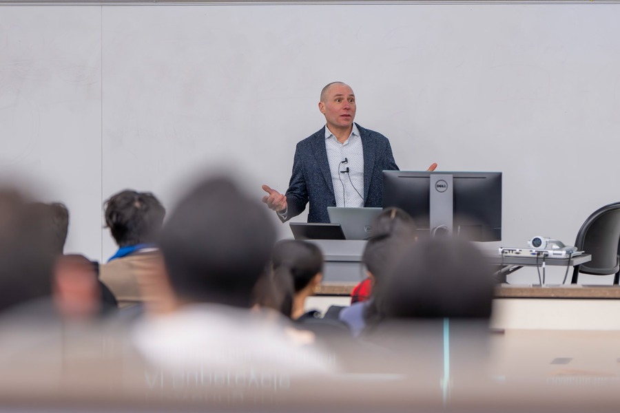
SDLP companies fund experiential learning programs, sponsor internships and send speakers to campus. The gateway course, "Changing the World with Chips," features industry speakers who provide first-year students with industry overviews and career pathways. Since 2022, over 900 students have taken this course.
"When we started this about four years ago, you could ask 100 students, and probably only four or five would know how their specific skills would apply to semiconductors," Esfarjani recalls. "Now it's just really inspiring to see the progress made and how semiconductors have become core part of engineering students’ interests at Purdue."
Hands-on experience at scale
Taylor Hartung, a Purdue alumnus at ASML, has witnessed how experiential learning transforms students. As a STARS program mentor and regular campus recruiter, he sees clear differences in Purdue candidates.
"Programs like STARS give students an edge because we know that they're familiar with these types of problems and that they've gone beyond the coursework to show they can think on their feet and work hands-on," Hartung explains.
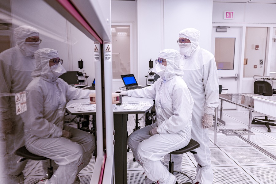
STARS students gain exposure to the lithography process and learn how components work together. “When STARS students come into our field, they already hit the ground running, understanding how hard it is, the challenges and the demand that’s put on the industry,” Hartung says.
Bartlett, who has seen STARS students visit GlobalFoundries’ facilities firsthand, is equally emphatic. “The STARS program was wildly successful in bringing students that weren’t sure they wanted to be in semiconductors in and getting them exposed to it,” he says.
Two Vertically Integrated Projects (VIP) courses anchor the experiential approach: System on Chip Extension Technologies (SoCET) focuses on chip design, while Semiconductors@Birck concentrates on manufacturing and advanced packaging.
The growth has been remarkable. SoCET expanded from approximately 40 students in 2022 to around 350 currently. Semiconductors@Birck, which started in 2023, now enrolls approximately 90 students.
"We have unique experiential learning programs that provide multi-semester, hands-on team projects addressing topics beyond typical classes," Janes explains. "While many experiential learning programs are difficult to scale, our frameworks are supporting relatively large numbers of students."
Students can also count corporate internships and study abroad courses toward certificate requirements, creating additional pathways to build technical and professional competencies.
My victory: From gateway course to Tokyo Electron
Leo Janert sat in his first "Changing the World with Chips" seminar as a junior in electrical engineering, listening to industry speakers describe the semiconductor field. The course opened his eyes.
"That seminar allowed me to learn more about what semiconductors really are and what it holds within industry," Janert recalls. "I found it interesting, and trying to get that foot into the industry, it is a bit of a learning curve. That's whyfor me, the certificate is allowing me to be better prepared for the industry."
Janert enrolled in the certificate program and began taking specialized courses. One sequence particularly resonated: ECE 50631, 50632 and 50633, exploring the physics side of semiconductors. "It's a great opportunity for students to have exposure to those topics and that kind of information that usually they want to have access to," he explains.
The VIP@Birck program became another cornerstone. "VIP brings out the opportunity for students to easily get into research," Janert says. In his first semester, he valued the clean room practices and learning from experienced team leaders and past STARS students.
But Janert's semiconductor education extended beyond West Lafayette. Through Purdue's Global Engineering Alliance for Research and Education (GEARE) program, he secured a hybrid internship with Tokyo Electron, a major semiconductor tool manufacturer. He spent two months in Hillsboro, Oregon, followed by one month in Sendai, Japan.
"Through that experience, I was able to get what it's like to work in a Japanese company that also has a pretty predominant presence within the US," Janert says. "That actual experience in industry as an intern will definitely help me once I do graduate and go find my first job."
This semester, Janert returned to Japan for study and work from January through August.
Beyond coursework and internships, Janert found community through the Semiconductor Student Alliance. "It's a great environment for students to learn from each other, see what research other students do within the club and see what companies are willing to come by onto campus," he says.
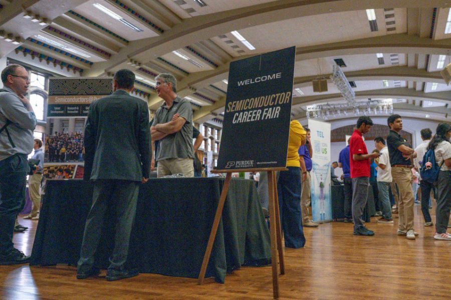
Purdue's semiconductor-specific career fair in fall 2025 drew 800 students.
Looking ahead to graduation, Janert plans to work in industry first, then pursue graduate studies within five years. "I believe whatever industry I find myself in would not veer far from semiconductors," he says. "The skills you develop through your classes and the way that you learn, those things will still help you when you graduate and continue on into wherever you find yourself."

Breaking the electrical engineering myth
When Hartung describes the talent ASML seeks, he quickly dispels a common misconception. "A lot of people think ASML or semiconductors are just looking for computer engineering or electrical engineering," he says. "That's not the case."
ASML's extreme ultraviolet lithography machines, which Hartung calls "the most complex machine that humankind has ever seen," require expertise across engineering disciplines.
"We need mechanical engineers who design a lot of the modules and precision components. We need physics to look at research and how we can tackle future problems. We need material science so that we can investigate new materials and how they interact," Hartung explains. "We need all these majors coming together in a symphony so that we can output these machines and create the next lithography components."
This multidisciplinary reality shaped the SDP from its inception. "Purdue took this challenge and really brought interdisciplinary departments together in close alignment with the faculties, whether it was industrial engineering, mechanical engineering, chemical engineering, electrical and computer engineering,” Esfarjani says.
As devices shrink and performance demands increase, challenges in thermal management, advanced packaging, materials science and manufacturing become as critical as circuit design.
"How you achieve high performance computing will require all kinds of innovative architecture," Esfarjani explains. "There's going to be device architectures in silicon for fabrication. Then there's going to be all kinds of innovations in the packaging of that silicon where you're bringing many chipsets from CPUs, GPUs, Memory and SOCs together in heterogeneous integration. Think of it like a bunch of Lego blocks that you put together to create a very high-performance, big chip."
What sets graduates apart
Hartung, who regularly interviews candidates from multiple universities, notices distinct advantages in Purdue SDP students.
"When we look at people coming into our company, programs like this give them an edge because we know that they're familiar with these types of problems," he says. The combination of technical coursework and hands-on experience creates graduates who understand both theory and practical constraints.
Industry participants at Purdue’s semiconductor career fair consistently express similar sentiments. “Industry participants were impressed with the students’ technical backgrounds and their knowledge of the industry,” Janes reports. “Other industry feedback reflects both strong technical preparation and valuable professional skills. The work ethic of our students is also valued by industry.”
Bartlett, himself an undergraduate chemical engineer who has spent 42 years working in semiconductors, looks specifically for students who bring non-traditional backgrounds to the field. “The fact that Purdue students show up with expertise in semiconductors from different backgrounds, whether that’s industrial engineering, chemical or mechanical engineering, we find highly distinguished and highly valuable,” he says.
Bartlett also points to the spark that experiential programs ignite. “People that get exposed to what semiconductors do, the degree of innovation that happens, and the unrelenting technical challenges — that is the spark,” he explains. “Once they get bit by that, they self-select to want to participate in the Purdue Semiconductor Degrees Program. Students who want to be in this because they’re excited by it are the best students when they end up in industry.”
For Hartung, the draw to Purdue runs deeper. "I love coming back to Purdue because it really is some of the best students around," he says. "Purdue is a Midwest gem. We intentionally go out of our way to come here."
Looking ahead
The program continues evolving to meet industry needs. "Our goals include updating and focusing our certificates and concentrations to align with the specific needs of companies in manufacturing, advanced packaging and chip design," Janes explains. "We also aim to significantly increase the number of students from departments most in demand for the various segments, with a particular focus on segments essential to re-shoring manufacturing and advanced packaging."
As artificial intelligence transforms the industries, the education curriculum is adapting. “AI is not going to be replacing humans, but it’s going to be a tool for humans that must be embraced to improve productivity,” Esfarjani explains. “The engineers must still understand the foundational principles such as physics, chemistry, circuits, thermodynamics, etc. They’re going to be using AI as a tool to solve even harder problems. They’re going to be very savvy with coding, math and statistical understanding. This is how curriculum should adapt.”
Bartlett sees even broader technological shifts on the horizon that make interdisciplinary preparation essential. “As we approach a $1 trillion semiconductor industry, the level of diversity of the technologies is remarkable,” he says, pointing to silicon photonics and quantum computing as areas gaining rapid momentum. “There are so many different technologies required to be successful for quantum. These are exactly the kind of areas where someone with a physics background, an optics background, or a materials science degree can cross over into semiconductors and bring highly valuable skills.”
"As part of Purdue's new AI competency initiative, we will also prepare students for utilizing AI in their respective fields," Janes adds.
The scale reflects Purdue's institutional commitment. "'Excellence at Scale' has been a Purdue focus, and certainly applies to our SDP," Janes says. "We are focused on filling a substantial portion of the talent needed by industry. The semiconductor industry is constantly innovating, and our students are well prepared to thrive and lead in this environment."
For Esfarjani, collaboration between industry and universities brings goal alignment for what is required. “Semiconductor industry has been built around innovation and innovation always comes down to people," he says. " This is what really enables each of those elements of this value chain to thrive."
His advice to students: "This is an amazing time to be in technology. Just pick your passion where you're most excited about and go drive it forward. Dream big, go after your ambitions. The industry is critically short of great talent, for people who think differently, who think out of the box, and who are willing to work hard and never give up.”
But success requires teamwork. Esfarjani invokes Michael Jordan: "Teamwork wins championships. Talent just wins games."
Hartung echoes this: “Be prepared for challenges. There’s plenty of complexity, but we need people that are willing to tackle it head on. We all count on each other to work every day, and it takes everyone pulling together to overcome these challenges.”
Bartlett’s advice is equally direct: “Just say yes. This is the time in your career and academic education to try new things and discover what you’re passionate about. Fall in love with this industry. It is a crazy, dynamic, ever-evolving industry — and it’s a wonderful place to spend your career.”
The SDP represents one component of the broader Semiconductors@Purdue initiative, which includes research centers and partnerships with companies establishing regional facilities: SK Hynix is building an advanced packaging facility, MediaTek has a design center and IMEC has an Indiana presence.
From Janert gaining international experience at Tokyo Electron to the 350 students now in SoCET to the 800 who attended the semiconductor career fair, momentum is building. Students understand semiconductors are foundational to everything digital. They've worked in clean rooms and designed chips. They've learned from industry mentors and collaborated across disciplines.
When they graduate and step into roles across the semiconductor value chain, they'll carry forward the Purdue tradition of producing engineers with strong fundamentals and the ability to adapt, innovate and lead.
"This is the best time to be in technology," Esfarjani says. "Dream big and pursue your passion. You're in a great program and you will have great days ahead of you."
For the 50,000 semiconductor engineers America needs, the pipeline runs through Purdue.
The SDP is a pillar of Purdue Computes, a strategic university initiative to further scale Purdue’s research and educational excellence in computing.
This story was developed as part of "Victories & Heroes: Your Campaign for Purdue." Join us in elevating Purdue Engineering education and excellence. Click here to be a part of Purdue history.