Birck Nanotechnology Center: 20th anniversary
Getting bigger and getting smaller
Nanotechnology is a rapidly developing field today, but it was still in its nascent stage 20 years ago when the Birck Nanotechnology Center was launched on October 8, 2005. Defined as the manipulation of matter at the nano scale, nanotechnology has burgeoned into a thriving domain, where the unique phenomena exhibited at its scale of between 1 and 100 nanometers have given rise to a host of applications across numerous economic sectors, particularly semiconductors, with the constant push to pack more processing punch into smaller footprints.
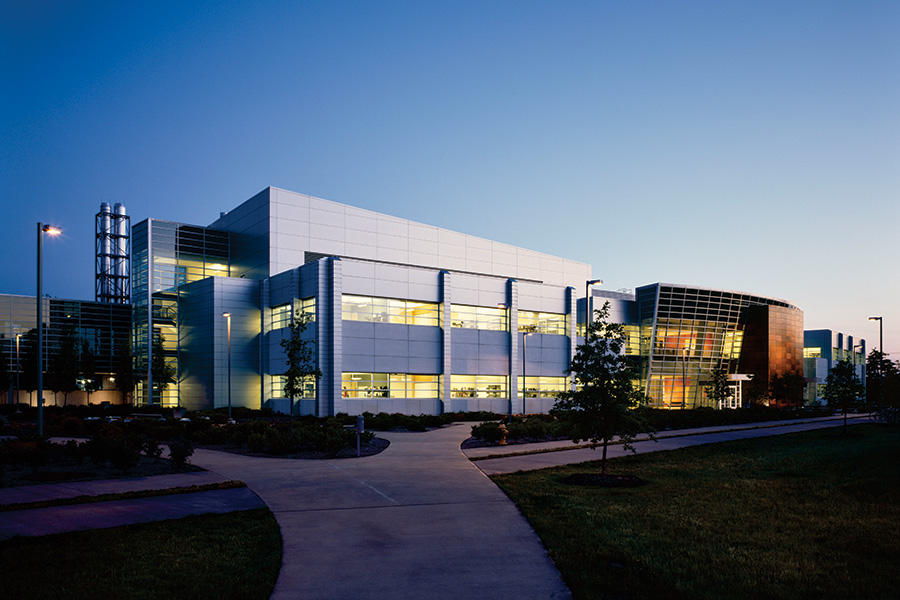
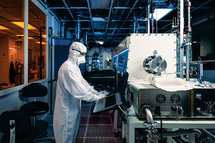
Birck has mirrored that growth, getting bigger and bigger as the nanotechnology domain shrinks ever smaller in the sizes it works at. From its modest origins in an antiquated laboratory in the Electrical Engineering building to today’s modern, state-of-the-art 186,000 square-foot facility with a 25,000 square-foot ISO class 3-4-5-6 nanofabrication cleanroom, it is now the home for Purdue’s advanced research and development on semiconductors, quantum science, and emerging technologies that manipulate materials and structures at the atomic scale.
Birck research is consequential and cutting-edge, always striving for that next step forward. As one of the flagship cleanroom facilities within the Midwest university network R1 Nucleus, funded by the Microelectronics Commons Program, Birck serves as a central hub for innovation. It is also a designated demonstration site for the SMART USA Institute to advance digital twin technologies for semiconductor processing, advanced packaging, and testing. The Atalla Institute for Advanced System Integration and Packing (ASIP) leverages Birck’s advanced packaging, fabrication and metrology capabilities in semiconductors. Birck supports the Scalable Asymmetric Lifecycle Engagement (SCALE), the preeminent U.S. program for semiconductor workforce development in the defense sector. The Purdue Quantum Science and Engineering Institute (PQSEI) at Birck discovers and studies new materials and basic physical quantum systems that can be integrated into future technologies.
In keeping with Purdue’s charter as a land-grant university, the Birck Nanotechnology Center is committed to its obligation to serve its home state of Indiana, as well as the broader needs of the country and world, by adapting to the changing needs of society through technology advancement and translation of that research to practice.
Birck’s mission is threefold, built around the principles of Educate, Innovate, and Collaborate. It strives to educate tomorrow’s leaders in research and technology; drive forward innovations in basic and applied research; and forge collaborations with public and private partners.
That includes offering multiple ways that industry partners can access the fabrication facilities and analytical capabilities. Their scientists and engineers can directly use the facilities and equipment; Birck engineers can work with partner technical teams to define, fabricate, and test new devices; samples can be submitted for Birck analysis and characterization; and partners can work with specific faculty on longer-term projects and sponsor graduate students to work on it.
Partners reap the benefit of the collaborative model that is the hallmark of Birck.
“Collaboration is greatly enhanced by sharing the same physical space in an environment that is purposefully designed to encourage ‘collisions,’” said Tim Sands, who served as director from 2006-2010. “I have worked in many interdisciplinary environments, but none has matched Birck. A critical feature was the lack of faculty ‘ownership’ of space or equipment so as to encourage collaboration and resist the entrenchment that eventually stifles vibrancy and impact.”
Collaboration is so widespread at Birck that Sands felt the need to chart it.
“To reinforce the importance of collaboration, I posted an annual collaboration network diagram on the walls of the lobby,” he said. “Each joint publication between research groups became a line segment connecting the nodes that represented each resident research group. In the early years of the Center, these network diagrams were sparse, but as the collaborative atmosphere intensified, annual network diagrams became very dense, with many nodes and connectors. These diagrams visually portrayed the value of being in the same space and sharing ideas and capabilities.”
A fresh start
Birck’s gestation came from Purdue’s realization of the importance of interdisciplinary, large-scale, team-based research. The result was Discovery Park, of which the first building was the Birck Nanotechnology Center. Discovery Park itself would originally consist of four research centers — nanotechnology, bioscience, e-enterprise, and entrepreneurship, all of which were aligned with Indiana’s economic development strategy — and over the years has expanded to include numerous other research institutes and centers that bring together researchers across disciplines to tackle large-scale global challenges.
When the idea for Birck first germinated in the late 1990s, nanotechnology — nano is a prefix meaning one billionth; a nanometer is one billionth of a meter — was an emerging science in which new materials and tiny structures are built atom-by-atom or molecule-by-molecule, instead of the more conventional approach of sculpting parts from pre-existing materials.
At the time, however, Purdue’s Electrical Engineering building sported an outdated solid-state lab. The “gowning area,” where you don the so-called “bunny suits,” was a public hallway, and once researchers donned their special protective clothing, they simply opened the door and stepped into a cleanroom. These facilities had been basically unchanged since the 1970s.

Then-Electrical and Computer Engineering (ECE) professor James A. Cooper approached the ECE Head David Landgrebe, who shared his concern. Cooper then reached out to professor Richard Schwartz, one of the original creators of the lab space, at the time serving as dean of engineering. Recognizing the urgency of the need, Schwartz brought it to the attention of then-President Steven Beering, setting the process in motion. Another ECE professor, Kent Fuchs, became the new ECE head and a strong champion of the vision, playing a vital role in identifying funding sources and gleaning learnings from the successes and setbacks of peer institutions.
Cooper worked with Schwartz in 1996 to form a team to review the existing capabilities and formulate a plan to bring the facilities in line with that of Purdue’s sister schools. Other ECE professors and the lab staff who ran the fabrication facilities and cleanroom were enlisted, a rough concept was developed, equipment lists were created, and the infrastructure necessary to support this equipment was determined with support from Beering. The team explored state, federal, industrial, and private funding sources.
Their groundwork revealed that the existing building could not support the needed infrastructure: Purdue needed a new building. It also became clear that the needs for the facility exceeded the ability of a single department. Planning for a new engineering building began in January of 1998, with a working title of the Purdue Interdisciplinary Nanofabrication Facility.
The mission statement: “To establish and construct a nanoscale technology facility that will lead the world in developing ultra small scale and ultra dense information processing technology used in knowledge and distributed intelligence systems. Simply, this facility will enable a new class of user-friendly personal information technology devices.”
Meeting a national challenge
Around that same time, on January 21, 2000, President Bill Clinton announced the National Nanotechnology Initiative (NNI), which provided a framework for nanotechnology research. This initiative continues to be funded, and to date has cumulative NNI funding of $45 billion.
Two overriding ideas emerged on center stage at Purdue: shared equipment and interdisciplinary collaboration. The value of both approaches was obvious to meet the needs of the Grand Challenges as set forth by the National Science Foundation. Without funding, however, the project was not really taken seriously by many faculty members.
At this point, Purdue had a new president, Martin Jischke. Cooper presented the concept to him, and he was enthusiastic about the idea. He said this new building idea dovetailed with a multidisciplinary research complex he envisioned for Purdue. Jischke would make this facility the centerpiece of the new complex that he would call Discovery Park.
“Martin Jischke saw how the research enterprise at Purdue was siloed,” said Arvind Raman, John A. Edwardson Dean of the College of Engineering. “He realized that what was missing for interdisciplinary research at Purdue was physical space where talents and ideas might intentionally and frequently collide. The vision for Birck grew from that.”
The idea of a new facility required a funding model beyond what Purdue had acquired in the past. Funding of the needed magnitude of $58.6 million involved contributions from the State of Indiana, the federal government, the university, and private donations.
Generosity at scale
Private donations loomed large in the funding equation. The creation of the Birck Nanotechnology Center was made possible by extraordinary philanthropic leadership from families whose generosity and vision continue to shape Purdue’s legacy in advanced research.
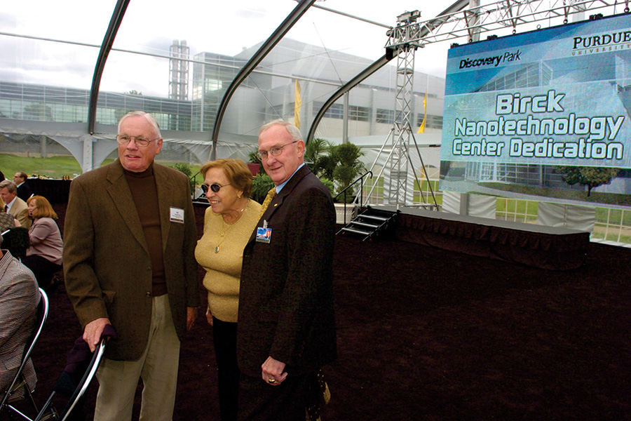
In 2001, three transformative gifts — $30 million from Michael and Katherine (Kay) Birck, $10 million from Donald and Carol Scifres, and $2 million from William B. and Mary Jane Elmore — laid the foundation for what would become one of the nation’s most advanced academic facilities for nanotechnology research.
Michael Birck, a 1960 graduate in electrical engineering, and his wife Kay had long been champions of Purdue. Michael served as a member of the Board of Trustees and held key leadership roles with the Purdue Alumni Association and the Purdue President’s Council. Their $30 million gift — the largest private donation in Purdue’s history at the time — not only made the nanotechnology center possible but firmly positioned Purdue at the forefront of a scientific frontier that promised to transform fields ranging from computing to medicine.
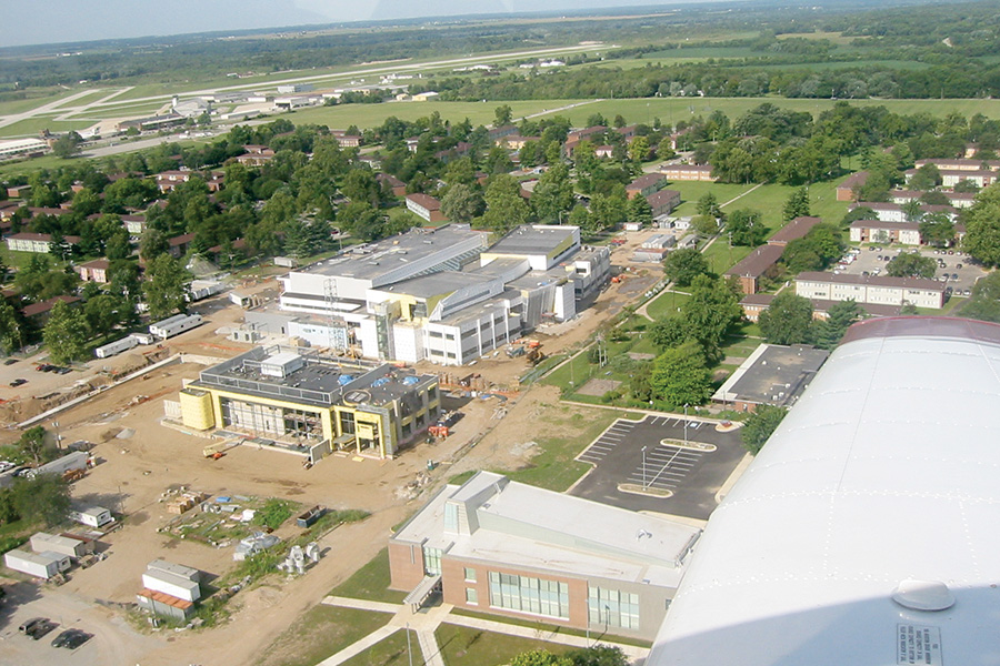
In recognition of their remarkable support, the center — then called ULTEC (Ultra-Large-Scale Integration and Technology Center) — was renamed the Birck Nanotechnology Center. The ceremonial groundbreaking in September 2001 launched Discover Purdue Week, which kicked off a yearlong campaign to highlight the university’s expanding research capabilities. Construction of the three-story, 186,000-square-foot facility began in summer 2002.
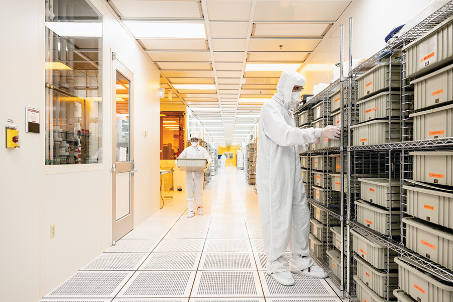
Alongside the Bircks, Donald and Carol Scifres — both Purdue alumni and Greater Lafayette natives — made a $10 million gift to support nanofabrication capabilities within the new center. Donald Scifres, a pioneering Silicon Valley entrepreneur with more than 130 patents, was co-chairman of JDS Uniphase Corporation and a Fellow of both the IEEE and the Optical Society of America. The entire cleanroom facility — one of the largest and most advanced in academia — was named the Scifres Nanofabrication Laboratory in honor of Donald’s father, Ray, who was an electrical engineering staff member for 35 yeras before retiring in 1975.
The gift from alumni William B. and Mary Jane Elmore went toward the center’s William and Mary Jane Elmore Advanced Wireless Concept Validation Laboratory. The School of Electrical and Computer Engineering was named after the family of William B. Elmore in recognition of an additional $25 million gift in 2021.
Together, the Bircks, Scifeses, and Elmores gave Purdue the resources — and the confidence — to lead in nanotechnology at a time when few universities had made such commitments. Their support enabled a facility with research capabilities unmatched in the academic world, accelerating Purdue’s emergence as a national leader in nanotechnology and beyond, and their foresight continues to shape the next generation of technological innovation.
Best in class
Today at Birck, electrical, mechanical, materials, chemical, industrial, and aeronautical engineers work alongside physicists, chemists, computer scientists, and biologists to devise structures and processes that utilize the unique features of the nanoscale. There are more than 140 faculty members at the center, representing 33 different academic departments across the Colleges of Agriculture, Engineering, Pharmacy, Science, Technology, and Veterinary Medicine.
The Birck Nanotechnology Center has become an example of excellence for other nanotechnology facilities around the world. It has been recognized with awards from international organizations, such as the prestigious “Lab of the Year” and “Cleanroom of the Year” awards. Further fulfilling its land-grant mission — creating a powerful economic ecosystem around the center’s strengths — Birck spurred a major project called Wabash Heartland Innovation Network (WHIN), during the directorship of professor Ali Shakouri.

Zhihong Chen stepped into the role of interim director of Birck in 2022 — the same year the U.S. CHIPS and Science Act was enacted, a pivotal moment for the nation’s semiconductor strategy. In 2023, Chen was appointed director, with a clear objective: to ensure that Purdue, and Birck in particular, would be well-prepared to contribute meaningfully to this once-in-a-generation opportunity and respond to emerging national priorities around semiconductors.
“As the largest and most advanced academic cleanroom and characterization facility in the country, Birck was already a critical asset,” Chen said. “Recognizing its strategic role, Purdue’s Board of Trustees approved a $49 million renovation plan that began in 2024. These upgrades were designed to support semiconductor, advanced packaging, and quantum research, enabling the continued development of a robust innovation ecosystem.”
Along with infrastructure support from the Silicon Crossroads Microelectronics Commons Hub (led by the Applied Research Institute) and the Lilly Endowment, as well as partnership with the SMART USA Institute, more than $75 million has been invested in the facility’s upgrades and new tools for processing and metrology. Birck is now well-positioned to advance the CHIPS Act’s goals — particularly in accelerating the lab-to-fab transition and supporting cost-effective prototyping of novel materials, devices, and processes in domestic facilities.
South Korea-based SK hynix Inc. is a believer in the Birck semiconductor ecosystem. The world’s leading producer of high-bandwidth memory chips, critical components of the graphic processing units (GPUs) that train AI systems, is investing more than $3.87 billion to establish a 430,000 square-foot facility at Purdue Research Park to support U.S. demand for semiconductors. The project will include work on advanced packaging and heterogeneous integration with Birck.
Virtual Birck
Birck is now incorporating digital twins and AI-driven — and even autonomous— research and development into both its infrastructure and daily operations. A key initiative is the development of “Virtual Birck,” which will allow students to learn and practice semiconductor fabrication and characterization in a virtual environment before entering the cleanroom. This will include an AI-powered chatbot designed to provide personalized, user-paced learning experiences.
This immersive approach democratizes access, enhances safety, boosts confidence, and accelerates learning. By enabling simulation, process iteration, and data analysis in the virtual space, it will significantly shorten R&D cycles and lower overall research costs.
“My vision is to make Birck the nation’s leading virtual twin-enhanced nanofabrication facility, where the physical and virtual worlds converge to shorten R&D cycles, reduce cost, and accelerate innovation,” Chen said. “What makes Birck uniquely positioned is not only our advanced capabilities, but the unified support from the university and the strength of our industry partnerships.”
Education mandate
In addition to advancing its technology profile, Birck plays an integral role in Purdue’s Semiconductor Degrees Program, which supports the national effort to train over 1 million additional skilled workers by 2030 and triple the number of STEM graduates. Purdue’s company-sponsored STARS program attracts students into the semiconductor field via intensive, industry-relevant projects, including manufacturing and advanced packaging projects in the Birck cleanroom and laboratories. A new STARS 2.0 program will leverage support from the Lilly Endowment and company sponsors to significantly increase program capacity, including academic year components in Birck laboratories. Students then build deeper expertise in Semiconductors@Birck, a Vertically Integrated Projects (VIP) program that enrolls engineering students from sophomore through senior year and has become the industry-fab–approved training pathway for future process, equipment, and process-integration engineers. Through multi-semester projects, students gain mastery of nanofabrication and semiconductor manufacturing concepts while also developing teamwork and project-management skills. Importantly, they make tangible contributions to ongoing Birck initiatives such as statistical process control (SPC) of nanofabrication processes and advanced packaging workflows. Most recently, a new VIP team, Virtual Twins@Birck, was launched to build digital twins of the Scifres cleanroom and its equipment, directly aligning with SMART USA Institute goals to democratize access to semiconductor education and training.
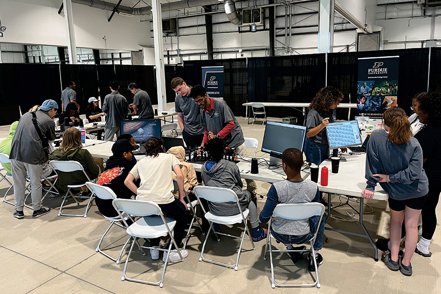
Birck hasn’t forgotten the children. Through the center’s K-12 program, Birck holds a variety of engaging events and facility tours to inspire tomorrow’s nanotech engineers and nanoscience researchers — a high priority of its mission is to develop students’ excitement about technology when they are young. Birck’s yearly outreach event, NanoDays, hosts an open house in its facility for more than 1,000 children in kindergarten through eighth grade. Birck recently brought its NanoDays outreach to the city of Lafayette’s Manufacturing Week, introducing elementary school students to nanotechnology.
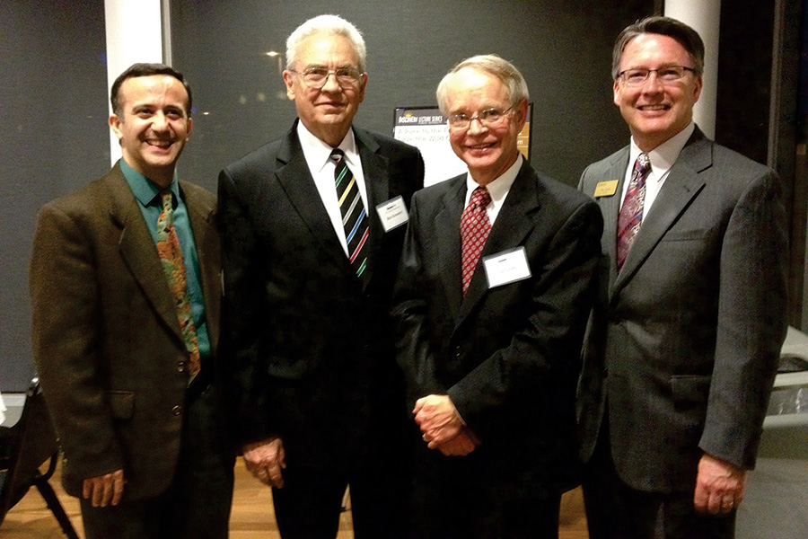
Credit for all this should be given to Birck’s leadership over the past 20 years: James Cooper and Richard Schwartz, founding co-directors from 2005-2006; Tim Sands, director from 2006-2010; Ali Shakouri, director from 2011-2021; and Zhihong Chen, interim director in 2022 and director from 2023 to present.
Their efforts have made Birck not only a leader in the field but a great place to work.
“Beyond its academic excellence, Birck fosters a unique sense of community,” Hudson said. “A facility like Birck can only achieve greatness through the commitment and daily efforts of the people who bring its mission to life. That pride and dedication are evident across the entire staff — from engineers and research scientists to the building support team, custodial staff, administrative personnel, and business operations.”
The information and photographs in this story are drawn from a forthcoming hardcover book, "Birck Builds the Future," by Purdue University Press. The book is available for preorder now.