International leaders in microelectronic systems, workforce development participate in inaugural Purdue workshop
More than 100 internationally acclaimed industry and academic leaders were in attendance at Purdue – largely in person — for the inaugural International Workshop for Advanced System Integration and Packaging (ASIP).
More than 100 internationally acclaimed industry and academic leaders were in attendance at Purdue – largely in person — for the inaugural International Workshop for Advanced System Integration and Packaging (ASIP).
Held in December, the event addressed “lab-to-fab” translation and workforce challenges for building future microelectronic systems. Discussion topics included system architectural and physical design enabled by multi-physics modeling tools, high-density interposers and substrates, process development for interconnect pitch scaling and thermal solution design — all while meeting reliability and manufacturing yield goals.
The workshop was organized by Purdue University's Atalla Institute for Advanced System Integration and Packaging (ASIP) in partnership with the Applied Research Institute (ARI), host of the Silicon Crossroads Microelectronic Commons Hub, imec USA, Cadence and Osaka University.
It brought together Integrated Device Manufacturers (IDMs), fabless and Electronic Design Automation (EDA) companies, equipment and tool vendors, materials suppliers, Outsourced Semiconductor Assembly and Test (OSAT) companies, national labs and university academics to describe current capabilities, identify future challenges and develop partnerships in pursuit of future programmatic opportunities. Senior technical leaders from SK hynix, IBM, AMD, imec, Intel and Joint2 Consortium of Japan highlighted advanced packaging drivers, capabilities, challenges and plans.
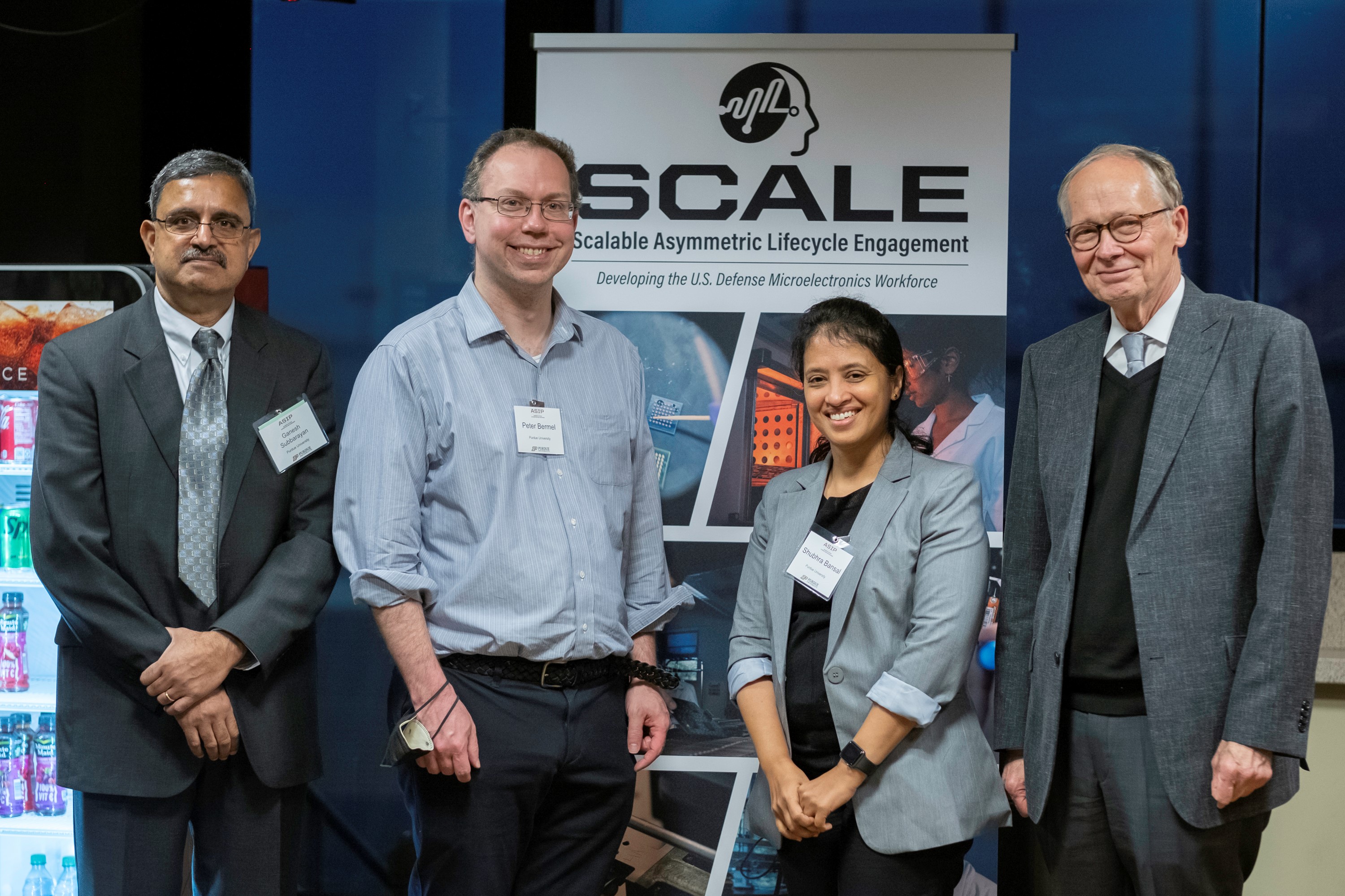
From left: Members of the ASIP team include Ganesh Subbarayan, the James G. Dwyer Professor of Mechanical Engineering and ASIP Director; Peter Bermel, the Elmore Professor of Electrical and Computer Engineering; Shubhra Bansal, associate professor of mechanical engineering and materials engineering; and Mark Lundstrom, the Don and Carol Scifres Distinguished Professor of Electrical and Computer Engineering and Purdue Chief Semiconductor Officer. Purdue University photo/Vincent Walter
The full agenda that includes topics and participants is on the event website.
The workshop highlighted Purdue’s ASIP capabilities and enabled partnerships between Purdue and U.S.-Japanese industries as well as between U.S. and Japanese industries themselves. These partnerships will serve as the basis for Purdue’s plans for national advanced packaging programs such as the DARPA Next-Generation Microelectronics Manufacturing (NGMM) program and the National Advanced Packaging Manufacturing Program (NAPMP). The workshop also enabled international exchange to inform crucial reshoring electronics packaging opportunities in the United States — which currently contains 3 percent of the global capacity.
“We were honored to host a very distinguished group of speakers and panelists at this inaugural international workshop. It was great to hear the leading industry experts describe the drivers as well as the challenges of advanced packaging at a pivotal time in the nation’s quest to re-shore a technology that has been lost over the past 30 years,” said Ganesh Subbarayan, the James G. Dwyer Professor of Mechanical Engineering and ASIP director.
Timothy Lee, Boeing Technical Fellow and 2024 IEEE-USA President-Elect, was one of the presenters on the Application Drivers and Advanced System Integration panel. “The topics covered by all of the speakers are relevant to advancing microelectronics/advanced packaging technologies to help re-shore semiconductor capabilities,” he said. “Also, the emphasis on workforce development is much needed.”
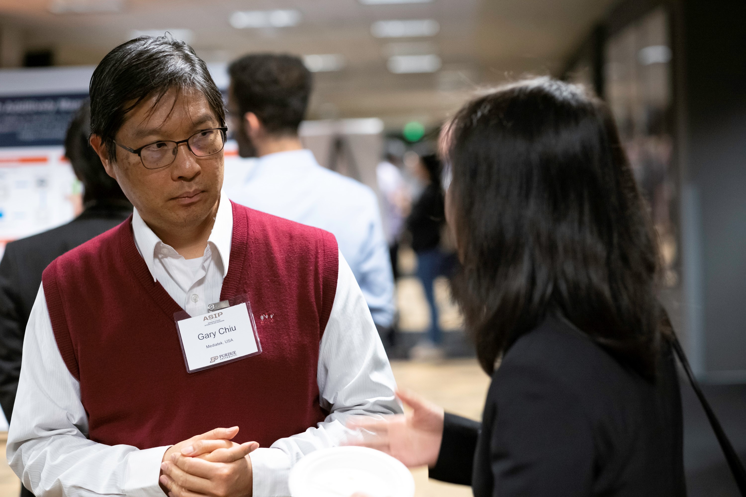
Gary Chiu, director of technology at MediaTek USA, listens to a presentation given by a Purdue Engineering student at the workshop. Purdue University photo/Vincent Walter
“Purdue University and the Attala Institute were delighted to host this important workshop at this critical time,” said Mark Lundstrom, the Don and Carol Scifres Distinguished Professor of Electrical and Computer Engineering and Purdue’s chief semiconductor officer. “ASIP was created to address both the research and educational challenges of complex, cross-cutting system-in-package integration to achieve performance, power and cost tradeoffs.”
About Microelectronics Research and Education at Purdue University:
The College of Engineering at Purdue University is ranked No. 4 in the United States and graduates more engineers than the top three ranked institutions combined. Purdue’s excellence at scale is exemplified by the many national and international microelectronic research centers at Purdue that have received more than $250 million in research funding. Specifically, in Advanced System Integration and Packaging, Purdue hosts five centers that together conduct nearly $90 million in research. Purdue University, through its expert faculty, is actively involved in guiding the formulation of the CHIPS Act R&D programs and is vigorously engaged with industry partners on all elements of CHIPS Act programs.
Complementary to the research mission, Purdue created the nation’s first MS degree program in semiconductors, with more than 55 Purdue faculty members teaching more than 100 courses on semiconductors and advanced packaging. Purdue’s educational innovations to motivate talented undergraduate students to pursue careers in semiconductors include the freshmen-level seminar course, “Changing the World with Chips — Introduction to Semiconductors,” and a unique eight-week hands-on experience in chip design and fabrication, “Summer Training, Awareness, and Readiness for Semiconductors.” More information is available.
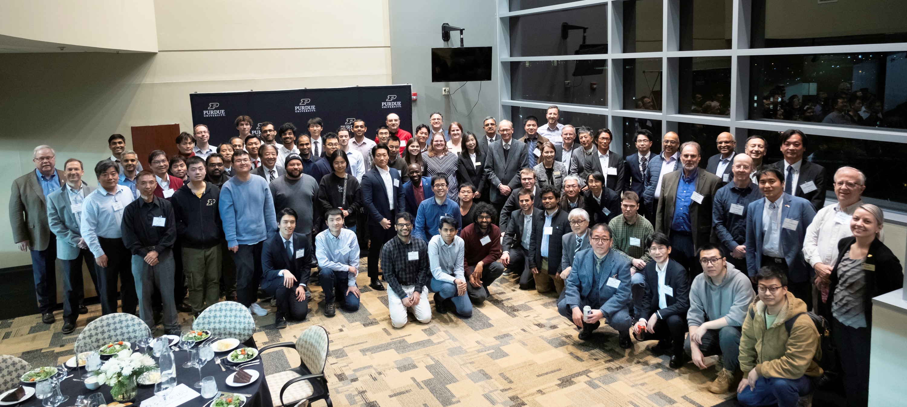
International Workshop for Advanced System Integration and Packaging (ASIP) at Purdue in December. Purdue University photo/Vincent Walter