Patterning Semiconductor Integrated Circuits with Holistic Nanolithography by Ronald Goossens and Anthony Yen
The first monolithic silicon integrated circuit was fabricated at Fairchild in 1961, a flip-flop containing 4 transistors. Fast forward the clock to 2022 and there was Nvidia’s H100 processor with 80 billion transistors fabricated at TSMC using its 4-nm-node technology. In this seminar, we will present a history of photolithography, the patterning technology that has fueled our industry’s progress for so many decades. Starting with contact/proximity printing, our industry gradually switched in the mid-1970s to projection lithography whose resolution is governed by the famous formula k_1 λ⁄NA, moving step-by-step to higher numerical apertures (NA) and shorter exposure wavelengths (λ) to provide better and better resolution. These two factors culminated in 193nm immersion lithography for which NA=1.35 and extreme ultraviolet (EUV) lithography at λ=13.5 nm. The k_1-factor has been driven down concurrently by better-quality projection optics, better metrology enabling advanced process-control schemes, and resolution-enhancing technologies driven by computational lithography to minimize CD variations and edge-placement error. These three factors (sounds so simple!), k_1 , λ , NA worked together to have made this remarkable journey possible. We will conclude the seminar with an outlook how continued advancements in EUV lithography, e-beam inspection, and computational lithography can work holistically to realize our vision of enclosing one trillion transistors in a single package by 2030.

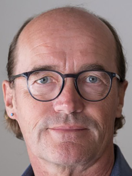
Ronald Goossens was born and raised in the Netherlands. After obtaining his PhD in physics at Utrecht University he joined Philips Research in the mid-1980s to work on the 3-micron CMOS device technology. After a 2-year industrial visitor sabbatical to Stanford University, he landed at National Semiconductor where he led a team that established analog circuit simulation as a core competency. An assignment at SRC as Science Director for Modeling and Simulation followed, bringing together the best brains from academia, industry, and the US DOE national labs to further fundamental understanding of semiconductor device physics. Next, he functioned as the program director for digital TV at NXP, resulting in the single-chip solution for the world’s first fully integrated multi-channel HDTV. In 2005 he joined ASML focusing on bringing computational lithography into semiconductor manufacturing. Today, after 17 years with ASML and culminating in the development of the 3-nm technology, he continues part time at ASML as Strategy Consultant for their Applications business line.

Anthony (Tony) Yen came to Purdue as a young immigrant to the US in the early 1980s. He received his BSEE here and went on to obtain SM, EE, PhD, and MBA at MIT. He began his career at Texas Instruments and was assigned to imec to co-develop advanced lithography technologies. From 1997 to 2017, apart from three years at Cymer (now part of ASML), he was with TSMC where he first led the development of its lithography processes, making TSMC the first company to adopt 193-nm lithography in the manufacture of logic integrated circuits, and then co-led infrastructure development for next-generation-lithography technologies on assignment at SEMATECH; in his last ten years of career at TSMC, he led the development of EUV lithography, including its mask technology, for high-volume manufacturing. In 2017 he joined ASML as Vice President and Head of Technology Development Center. He is a recipient of the Frits Zernike Award for Microlithography from SPIE and the Outstanding Electrical and Computer Engineer Award from Purdue. He serves on Purdue’s Semiconductor Degrees Leadership Board.


