Purdue researchers develop new technique to boost overall brightness of spin defects in hexagonal boron nitride
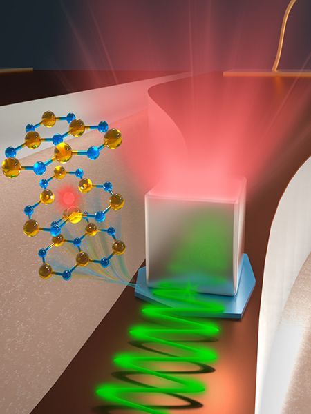
Researchers with the Birck Nanotechnology Center and Elmore Family School of Electrical and Computer Engineering at Purdue University have developed a technique to improve the overall brightness of the negatively charged boron vacancy (VB–) in hexagonal boron nitride (hBN). Researchers observed overall enhanced emission of 250 times by coupling the defect with silver-based nanopatch antennas (NPAs), making it much easier for researchers to use VB– defects in practical quantum sensing applications like measuring magnetic fields, pressure, temperature, and nuclear spins with extreme sensitivity. These measurements are key to advancing life-changing technologies, including medical imaging, cell phones and radar communications, and navigation systems.
Their findings were published in the paper “Greatly Enhanced Emission from Spin Defects in Hexagonal Boron Nitride Enabled by a Low-Loss Plasmonic Nanocavity” in November 2022 in the scientific journal NANO Letters by the American Chemical Society.
Researchers in the field of quantum sensing have studied the VB– spin defect in hBN in recent years and its ability to preserve spin coherence even when implanted at nanometer distances from hBN’s surface. The advantage of this defect in hBN is its potential use as an ultra-thin quantum sensor, able to take extremely sensitive measurements at nanometer scale from other materials. Unfortunately, VB– defects have a downside. They are limited by poor optical quantum efficiency. In other words, the light they emit while measurable is too dim to be used in interactive applications.
Previous studies coupled VB– defects with NPAs— used to enhance the transmission of light through metal film— and gold film to boost brightness. However, these demonstrations resulted in enhanced brightness up to only 17 times. That’s still not bright enough to be used in interactive applications, said Xiaohui Xu, a doctoral student of materials engineering and co-author of the paper.
“In the wavelength this emitter emits, silver is better than gold,” Xu said. By coupling VB– with a carefully designed and assembled NPA using silver film, they enhanced brightness more than 15 times compared to studies using gold film. In the paper, researchers reported an overall brightness enhancement of 250 times, making it much easier to use in practical sensing applications.
“Atomic thickness of hBN enables exceptionally high sensitivity in probing critical material properties and, in parallel, the close proximity to the probed object,” said Vladimir Shalaev, the Bob and Anne Burnett Distinguished Professor of Electrical and Computer Engineering and corresponding paper author. “Importantly, the demonstrated strong enhancement of photoluminescence in hBN dramatically increases the efficiency of the optical channel that can provide valuable information about quantum materials.”
With such improved brightness, VB– defects can be used as ultra-thin quantum sensors, but that’s not all. Xu said their technique could help isolate single VB– defects, which, so far, have been too dim to separate from their clustered form. When obtained, the single photon emitters can be useful in even more quantum applications, including quantum computing.
Quantum sensing is ready to play a critical role in helping to solve modern problems, said Abishek Solanki, a doctoral student of electrical and computer engineering and co-author of the paper. While it’s not the most talked about area of research outside of its scientific community, Solanki said it’s a hidden gem in the field.
“Quantum sensing is ready to help accelerate material science development and understanding of materials at a very small scale, with very high time and spatial resolution,” he said. “In that sense, I think quantum sensing is the hidden gem, or more under-appreciated gem, out of these jewels [in quantum technologies].”