New material advances lead to smaller and better-performing transistors
A team of researchers from Purdue University’s Elmore Family School of Electrical and Computer Engineering have developed a way to achieve smaller and higher-performing transistors. Led by Peide Ye, the Richard J. and Mary Jo Schwartz Professor of Electrical and Computer Engineering, the group has been seeking to exploit materials much thinner than silicon to meet that goal.
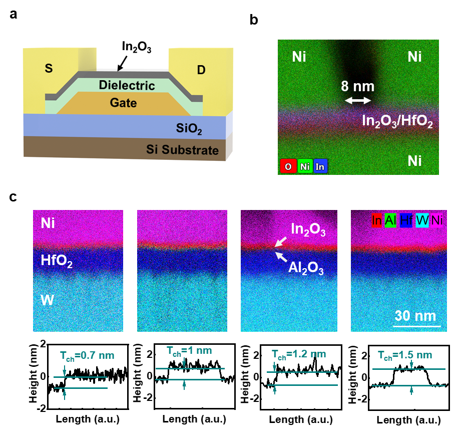
Ye’s research group specializes in atomic layer deposition (ALD) technique and its integration on semiconductor materials. ALD is a surface controlled layer-by layer process for the deposition of thin films with atomic layer accuracy. The major innovation of this work is to use atomically thin indium oxide grown by ALD as the semiconductor channel with superior device performance.
New advances in this area, outlined in a paper published in Nature Electronics, involve the scaling of both the dimensions of the semiconductor materials and the size of the transistor. Ye says further scaling of silicon-based devices and the development of alternative semiconductor channel materials that are compatible with current fabrication processes are challenging. This paper, though, reports high-performance ALD indium oxide transistors with channel length down to 8 nm, channel thickness down to 0.5 nm, and equivalent dielectric oxide thickness (EOT) down to 0.84 nm. He says these numbers are all the smallest among all oxide semiconductor transistors with current of 3.1 A/mm at voltage of 0.5 V. It exceeds any other related oxide semiconductor work.

Ye says the approach provides a promising alternative channel material for scaled transistors with back-end-of-line (BEOL) compatibility, compared with both established and emerging material and device technologies.
In addition to Ye, researchers involved in this work include Mengwei Si, postdoctoral researcher, Zehao Lin, PhD student, Zhizhong Chen, postdoctoral researcher, Xing Sun, former PhD student in Wang’s group, and Haiyan Wang, Basil S. Turner Professor of Engineering.
This work was supported by the SRC nCore IMPACT Center, Air Force Office of Scientific Research, and SRC/DARPA JUMP ASCENT Center.