Karla L. PerezThe University of Texas at El Paso Project Title: Alloy Thin Films by Multi-target Sputtering
|
 |
Introduction
Thin films can be described as generically coatings that are larger in 2D than in 3D. They are often used in a wide variety of technological applications due to the manageability of their properties which include compositional variation and grain boundary configuration. Thin films are often deposited by a process in which atoms in a target are ion bombarded and then compiled onto a substrate; this process is called sputtering. Sputtering will be used to deposit pure and alloy thin films using different targets such as copper, nickel, titanium and silver as a basis for this research project.Project Objectives
- The main goal is to create alloy thin films with uniform composition and thickness.
- Design a system which will enable us to manage the composition and geometry of the alloy thin film.
Experimental Approach
- Deposit pure metal films by sputtering in order to find the ratio at which the film is deposited and the thickness of the film.
- Mask the film to be able to measure its thickness.
- Measure the film thickness using different approaches; for instance atomic force microscope (AFM), profilometer and optical microscope.
- Deposit the alloy thin films also by sputtering. The alloy target used is one of Cu and Ag.
- Measure the composition of the film using the scanning electron microscope (SEM).
Research Findings
- Using an optical microscope to measure the thickness of the pure metal films only gave a rough idea of its thickness and not an actual measurement. The optical microscope had to be in DIC (Differential Interference Contrast)
- Due to the thinnest of some films the profilometer did not give an accurate measurement of the film thickness; for instance molybdenum.
- The AFM (Atomic Force Microscope) provided the best reading of the thickness of the film compared to all the techniques used before.
- The mask used when depositing the film created a shadow implying that the atoms were not deposited perpendicular to the substrate but with a slope alongside the mask.
- Finally, a scratch in one of the film allowed us to have a good measure of the film thickness; from there on we purposely created scratches on the film and measured the thickness from there.
- Unlike films such as molybdenum and copper the silver films made it relatively easy to find its thickness using the AFM because they did not scatter when creating the scratch.
- Copper films were deposited using a scotch tape mask which allowed it to measure its thickness because the shadow was very thin.
- The films deposited were thicker in the center of the substrate.
- When measuring the composition of the alloy thin films we realized the importance of the position in which the film is sputtered because that allowed us to control the way the atom will be deposited.
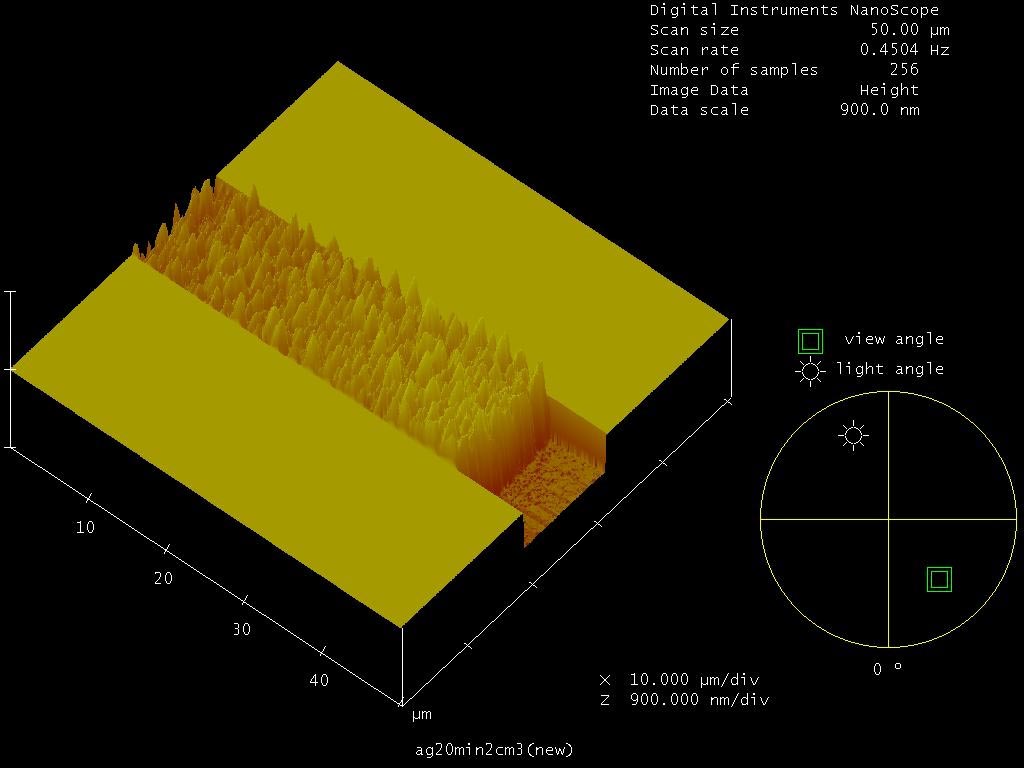 Figure 1: Ag film deposited for 20minutes, 2cm apart from the target |
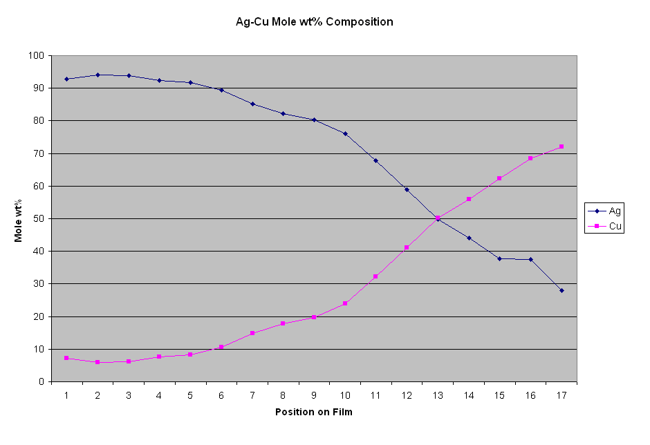 Figure 2: Mole Composition of a Ag-Cu alloy thin film |