Bi2Te3 Nanowire Array/Epoxy Composites for Thermoelectric Power Generators
by Kalapi G. Biswas and Timothy D. Sands
Introduction
Templated nanowire arrays[1-4] of thermoelectric materials have attracted attention over the last decade due to their potential application in the low cost, high yield fabrication of thermoelectric elements with lengths in the range of tens to hundreds of microns. In addition to offering the advantages of nanowire materials, the composite provides an opportunity to engineer structurally robust materials necessary for the fabrication of multi-couple integrated devices. The thermal conductivity of the composite is controlled by the matrix thermal conductivity and volume fraction; thus, the effective thermoelectric figure-of-merit (ZT) of the nanowire array composite will be reduced relative to that of the thermoelectric nanowire material alone. The objective of this study is to investigate and optimize the fabrication parameters influencing the composite’s ZT in order to achieve a power conversion efficiency goal of 20% and power density of ~ 104 W/m2.
The most promising materials systems for direct thermal energy converters as observed in bulk and thin-film materials and multilayer nanowires[5, 6] are based on Bi2Te3 and PbTe at the low and high ends of the operating temperature range, respectively (50-550°C). In this study, the Bi2Te3 materials system was chosen to cover the low temperature range (50-200°C). The porous anodic alumina (PAA) template used for the nanowire synthesis has a thermal conductivity (к) of 1.7 W/m-K[7], which is comparable to that of the Bi2Te3 nanowire array[4, 8]. Thus, the PAA matrix provides a parasitic thermal shunt for thermoelectric power generation devices and needs to be replaced with a lower thermal conductivity material. A commercially available epoxy resin SU-8, which is widely used in the microelectronic industry for high aspect ratio and 3-D lithographic patterning was chosen for infiltrating the nanowire array. It is also used as a permanent and functional material in silicon-on-insulator technologies[9, 10]. The thermal conductivity of epoxy resin SU-8 ( к=0.2W/m-K) is an order of magnitude lower than that of the PAA matrix with a degradation temperature of ~ 380˚C[9] and hence can be used effectively over the low temperature range for thermoelectric applications.
In addition to reducing the effective thermal conductivity of the composite, a minimum thermo-element thickness (>10um) is required to maintain the temperature difference and to overcome the effects of joule heating due to contact resistance. In this report, we have demonstrated a process for fabricating high aspect ratio (200:1), dense (~75% volume fraction) self-supporting Bi2Te3 nanowire array/SU-8 composites with high structural integrity and low effective thermal conductivity.
Nanowire array fabrication and characterization
The Bi2Te3 nanowires were synthesized by galvanostatic electrodeposition into porous anodic alumina (PAA) template. The templates were pore widened using 3 wt% KOH/ethylene glycol solution for achieving 75% porosity. The electrolyte solution[2] consisted of 0.035 M Bi (NO3)3.5H2O (Alfa Aesar, 99.999%) and 0.05 M HTeO2 (Te, Alfa Aesar, 99.999%) in 1M nitric acid and a pH=1 was maintained throughout the process. The nanowires were electrodeposited at 5mA/cm2 with 3 second pulses. The resulting nanowires were ~50 μm in length, corresponding to a growth rate of ~5nm/s. Following synthesis, the nanowire arrays were mechanically planarized to overcome any overgrowth or non-uniformity in nanowire lengths[11]. The Figure 1 presents the field-emission scanning electron microscopy (FESEM) images of planarized Bi2Te3 nanowires embedded in PAA template. The top view exhibits dense nanowire array ~75% volume fraction coverage and the side view reveals the high aspect ratio ~200:1.
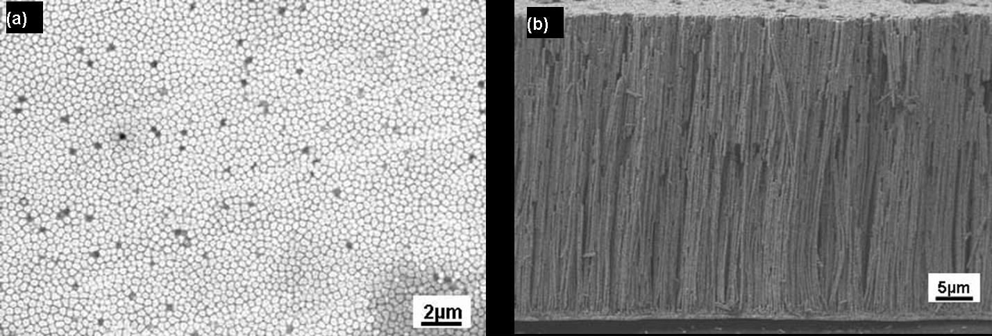
Figure 1: FESEM image of Bi2Te3 nanowire array composite (a)top view exhibits dense nanowire array (75% volume fraction) and (b)side view reveals high aspect ratio (200:1)
X-ray diffraction and transmission electron microscopy analysis presented in showed that the nanowires have <11.0> texture, the orientation that yields the highest ZT in single crystals. Compositional analysis carried out by energy dispersive spectroscopy (EDS) confirm the stoichiometry of the nanowire array as Bi:Te at.% ~40:60.
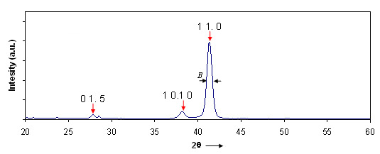
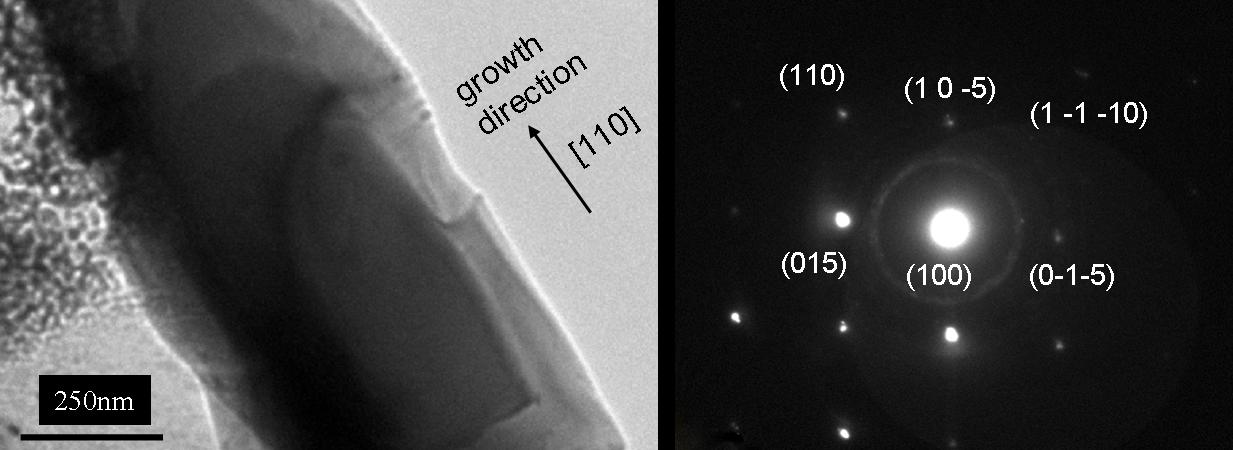
Figure 2: (a) X-ray diffraction pattern for Bi2Te3 nanowire array embedded in PAA and (b)TEM analysis: (left) bright field image of Bi2Te3 nanowire indicating <110> growth direction and (right)corresponding selected area electron diffraction (SAED) indicating single crystalline nanowire
SU-8 matrix infiltration
For fabricating the nanowire array/SU-8 composite, the PAA template is entirely removed by etching in a 3 wt% KOH solution for 24 hours. To prevent collapse of free-standing Bi2Te3 nanowires as a consequence of capillary forces acting on nanowire sidewalls, the rinsing procedure with de-ioinized water (72mNm-1) is followed by lower surface tension solvent, isopropanol (21.8 mNm-1). This procedure yields 40-micron-thick self-supporting planarized Bi2Te3 nanowire arrays. SU-8 is then spin-coated on the nanowire array at 2000 rpm to obtain a resin matrix thickness of 40μm, UV processed at ~360nm and baked. To accommodate the large SU-8 thickness, all baking steps are carried out on a leveled hotplate (by conduction) to avoid dried layer formation on the surface, hindering diffusion of solvent from the interior.
The SU-8 epoxy infiltration, adhesion, and mechanical integrity were investigated by fracturing the nanowire array/epoxy composite. A cross-sectional view of the nanowire array/ epoxy composite structure is presented in Figure 2, which shows nanowires completely embedded in the polymer matrix with a crystallographic cleavage plane evident in the Bi2Te3. The fracture proceeds by crack propagation through the nanowire, suggesting that the SU-8/nanowire interface is of high structural integrity.
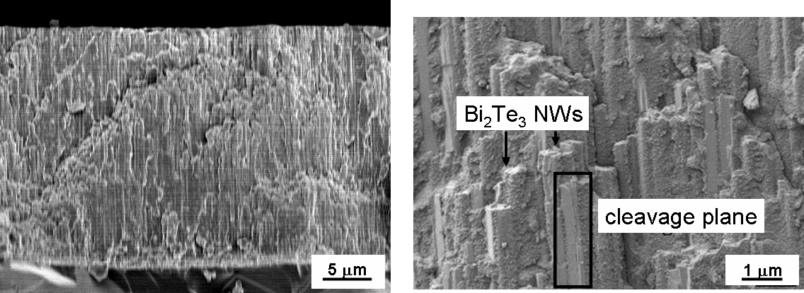
Figure 3: Fractured nanowire array/epoxy composite showing (left) nanowires completely embedded in epoxy matrix, and (right) expanded view showing cleavage plane in nanowire.
The crystallographic cleavage plane observed in the fractured nanowire array composites can be attributed to the weak van der Waals bonding between the Te-Te atomic planes in Bi2Te3 crystal structure[15, 16].
Conclusion
We have demonstrated the fabrication of dense (75% nanowire volume fraction), 40μm thick, high aspect ratio (200:1), structurally robust Bi2Te3 nanowire array/ SU-8 composite for thermal energy converters. The galvanostatic electrodeposition method in PAA template enables high-rate growth of single-phase, crystalline <11.0> oriented Bi2Te3 nanowires at room temperature. This orientation yields the highest ZT in single crystals. The PAA template, which produces a parasitic thermal shunt, was replaced successfully with a low thermal conductivity material, SU-8 (0.2 W/m-K). The highest effective thermoelectric figure-of-merit (ZTcomp) of the composite can be achieved by optimizing the matrix thermal conductivity and volume fraction while maintaining structural integrity. We also demonstrated an optimized composite structure with low matrix thermal conductivity of 0.2W/m-K and volume fraction of 25%. The SU-8 infiltration in the nanowire array, adhesion to the nanowire sidewalls, and mechanical integrity of the composite structure were confirmed from the fractured composites.
Acknowledgement
This work was supported by a grant from the Office of Naval Research (N000140610641). The authors would like to thank Vijay Rawat for TEM analysis, Prof. Jeff Youngblood (Purdue University) for his insight on techniques of polymer infiltration in nanowire arrays and Jeremy Schroeder (Purdue University) for his expertise in SU-8 epoxy resin.
References
M. S. Sander, R. Gronsky, T. Sands and A. M. Stacy, Structure of Bismuth Telluride Nanowire Arrays Fabricated by Electrodeposition into Porous Anodic Alumina Templates, Chem. Mater. ,2003, Vol 15, p 335-339
C. G. Jin, X. Q. Xiang, C. Jia, W. F. Liu, W. L. Cai, L. Z. Yao and X. G. Li, Electrochemical fabrication of large-area, ordered Bi2Te3 nanowire arrays, Journal of Physical Chemistry B,2004, Vol 108 (6), p 1844-1847
A. R. Abramson, W. C. Kim, S. T. Huxtable, H. Yan, Y. Wu, A. Majumdar, C.-L. Tien and P. Yang, Fabrication and Characterization of a Nanowire/Polymer-Based Nanocomposite for a Prototype Thermoelectric Device, Journal of Microelectromechanical Systems,2004, Vol 13 (3), p 505
D.-A. Borca-Tasciuc, G. Chen, A. Prieto, M. S. Martín-González, A. Stacy, T. Sands, M. A. Ryan and J. P. Fleurial, Thermal properties of electrodeposited bismuth telluride nanowires embedded in amorphous alumina, Applied Physics Letters,2004, Vol 85 (24), p
R. Venkatasubramanian, E. Siivola, T. Colpitts and B. O'Quinn, Thin-film thermoelectric devices with high room-temperature figures of merit, Nature,2001, Vol 413 (6856), p 597-602
T. C. Harman, P. J. Taylor, M. P. Walsh and B. E. LaForge, Quantum Dot Superlattice Thermoelectric Materials and Devices(Report).
D. A. Borca-Tasciuc and G. Chen, Anisotropic thermal properties of nanochanneled alumina templates, Journal of Applied Physics,2005, Vol 97 (8), p
J. H. Zhou, C. G. Jin, J. H. Seol, X. G. Li and L. Shi, Thermoelectric properties of individual electrodeposited bismuth telluride nanowires, Applied Physics Letters,2005, Vol 87 (13), p
A. d. Campo and C. Greiner, SU-8: a photoresist for high-aspect-ratio and 3D submicron lithography, Journal of Micromechanics and Microengineering,2007, Vol 17, p R81-R95
E. H. Conradie and D. F. Moore, SU-8 thick photoresist processing as a functional material for MEMS applications, Journal of Micromechanics and Microengineering,2002, Vol 12, p 368-374
K. Biswas, Y. Qin, M. DaSilva, R. Reifenberger and T. Sands, Electrical properties of individual gold nanowires arrayed in a porous anodic alumina template, physica status solidi (a),2007, Vol, p 1- 7
W. Dai, K. Lian and W. Wang, A quantitative study on the adhesion property of cured SU-8 on various metallic surfaces, Microsyst Technol,2005, Vol 11, p 526-534
MicroChem, SU-8 Table of Properties, in http://www.microchem.com/resources/app_notes.htm.
R. L. Barber, M. K. Ghantasala, R. Divan, K. D. Vora, E. C. Harvey and D. C. Mancini, Optimisation of SU-8 processing parameters for deep X-ray lithography, Microsystem Technologies 2005, Vol 11, p 303-310
G. E. Shoemake, J. A. Rayne and J. R. W. Ure, Specific Heat of n- and p-Type Bi2Te3 from 1.4 to 90°K Physical Review,1969, Vol 185 (3), p 1046
M. H. Francombe, Structure-cell data and expansion coefficients of bismuth telluride, Br. J. Appl. Phys.,1958, Vol 9 p415-417