
Purdue ECE takes semiconductor training on the road with mobile fabrication lab
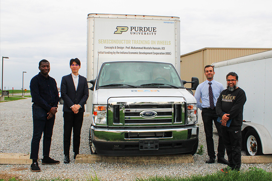
A compact lab developed at Purdue is giving students and aspiring semiconductor technicians hands-on experience with chipmaking equipment without requiring access to a multimillion-dollar cleanroom.
Most people who want to learn how computer chips are made cannot simply walk into a semiconductor fabrication facility.
Traditional cleanrooms are expensive to build and operate, access is tightly controlled, and students often must complete extensive safety and facility training before they can get near the equipment. For researchers, those requirements are necessary. For someone learning the basic steps of semiconductor manufacturing, they can create a major hurdle.
A team in Purdue University’s Elmore Family School of Electrical and Computer Engineering is working on a different approach: Take the training lab to the students.
Led by Purdue ECE Professor Muhammad Hussain, the Mobile Semiconductor Fabrication Lab, or Mobile Fab, puts many of the fundamental tools and processes used to make semiconductor devices into a compact, portable training environment. The goal is not to replace the sophisticated cleanrooms used to manufacture advanced chips. It is to give more people an opportunity to understand how semiconductor fabrication works.
“We rarely come across a clean room that is dedicated to training or education only,” said Min Sung Kim, a Purdue ECE PhD student who has served as a teaching assistant for the school’s IC and MEMS Fabrication course, which enrolls an average of approximately 120 students each year.
Research facilities have expensive equipment and strict procedures designed to protect experiments and devices, Kim said, making access difficult and costly for students who need to learn the underlying processes.
With the Mobile Fab, the priority shifts from producing a pristine device to understanding what each piece of equipment does and why each step matters.
“Gowning, cleanliness and safety procedures are essential in semiconductor manufacturing,” Kim said. “The Mobile Fab complements conventional cleanroom training with simpler gowning and cleanliness requirements suited to introductory lessons. It maintains appropriate safety measures while helping students learn how fabrication equipment works and why each process step matters.”
Kim, originally from South Korea, is pursuing his PhD in advanced packaging and heterogeneous integration for flexible CMOS electronic systems.
Chipmaking through hands-on learning
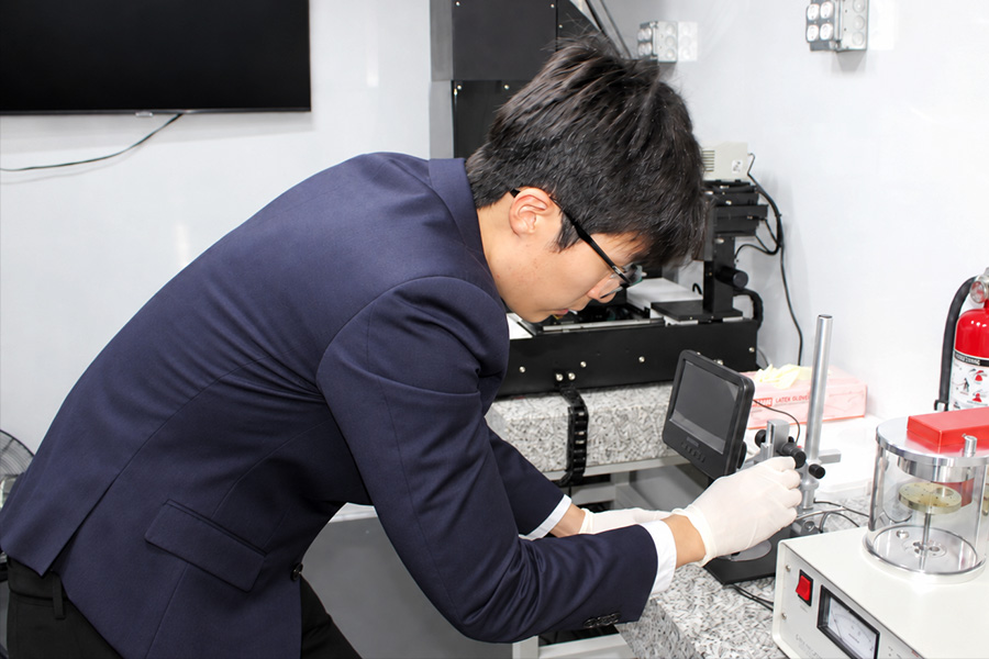
Semiconductor manufacturing involves building extremely small structures on a wafer, one layer and pattern at a time. The Mobile Fab gives trainees experience with several of those basic processes.
One is lithography, which transfers a circuit design onto the surface of a wafer. In simple terms, a design created on a computer becomes a physical pattern used to build electronic devices. Hussain describes the transformation simply: turning “bits to atoms.”
Purdue ECE PhD student Yusuf Adebakin demonstrated the lithography process.
“Lithography can seem very abstract until you see the process happen in front of you,” Adebakin said. “Being able to follow the steps on the equipment helps connect the design you see on a computer with the physical structures that eventually become part of an electronic device.”
Adebakin, originally from Nigeria, joined Purdue ECE in fall 2023 and continued into the PhD program after completing his master’s degree. His research focuses on extreme large-scale heterogeneous integration, exploring new approaches to combining complex electronic devices across large areas and unconventional shapes and surfaces.
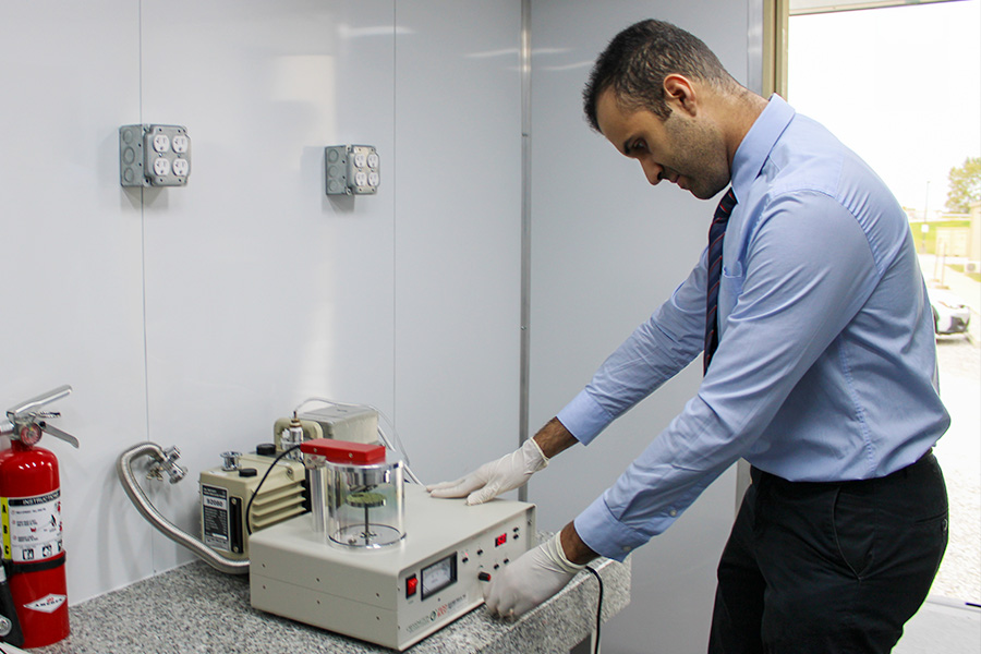
Another tool, called a sputter coater, deposits an extremely thin layer of material onto a surface. Purdue ECE PhD student Dhiya Belkadi explained how the tool uses plasma, an energized gas, to dislodge material from a target so it settles onto a sample. The lab system was configured to deposit a thin layer of gold.
“It’s one thing to learn these processes from a diagram or a lecture, but it’s different when you can operate the equipment and actually see what is happening,” Belkadi said. “The Mobile Fab makes those concepts much more real and gives students a better sense of how semiconductor fabrication works in practice.”
Belkadi, originally from Algeria, studies the physical limits of heterogeneous integration, working to understand what happens as electronic systems are combined at increasingly smaller scales.
Other Mobile Fab tools introduce trainees to processes such as etching, which removes material to create tiny features, and deposition, which applies layers of material.

Designed to travel
The Mobile Fab is designed to address one of the biggest barriers to semiconductor education: access.
Instead of requiring students to travel to universities, companies or national laboratories with specialized cleanrooms, the lab can take semiconductor fabrication equipment to schools and communities.
“Our goal is to expose the students, a wider group of students, to semiconductor manufacturing technology and equipment,” Kim said. “By utilizing this truck, we can access wider audiences.”
The current platform occupies roughly a 12-by-8-foot space, about 100 square feet. Hussain estimates that creating a conventional cleanroom of similar size with comparable equipment could cost about $2 million. He believes the portable approach could be reproduced for roughly $500,000.
The initial Mobile Fab concept envisioned semiconductor training inside an 18-wheeler. Hussain said the current system is a starting point the team can refine, with future versions possibly expanding to larger vehicles.
Making fabrication mobile also required the team to rethink the cleanroom itself.
Conventional facilities tightly control particles, temperature, chemicals and other environmental conditions across an entire room. The Mobile Fab instead focuses environmental control on the smaller area around the device or process. Its equipment also operates sequentially rather than all at once.
Safety is central to the design. The Mobile Fab avoids liquid chemicals and uses lower-hazard alternatives where possible. For example, one lithography process uses visible LED light instead of ultraviolet light. The exposure takes longer, but trainees can still learn the principles behind the process.
The equipment also must endure something traditional cleanroom tools rarely encounter: potholes.
The team worked with Purdue groups including Health and Safety, transportation, vehicle maintenance and research machining services to secure and protect sensitive equipment while the lab is on the road.
Building a training pipeline
The Mobile Fab is one part of a broader approach that blends online, virtual and hands-on learning.
Central to that effort is the Veterans Inclusion and Competency Toward Semiconductors, or VICTORS, program, which Purdue developed to prepare veterans for semiconductor technician careers.
Participants first learn semiconductor basics, cleanroom safety and fabrication processes through Purdue Online. They can then practice those concepts using VFAB, Purdue’s virtual chip fabrication simulator, before moving to hands-on training.
Hussain compares vFabLab to the flight simulators pilots use before entering a cockpit. Trainees can become familiar with semiconductor devices and the fabrication sequence before working with the real tools.
“If we use this kind of virtualization and then bring the trained people into the physical space, they are far more aware, fully ready and can actually get things done at a very fast pace,” Hussain said.
Purdue’s online introductory semiconductor fabrication course has recorded more than 20,000 enrollments in a little more than two years, Hussain said. VFAB has attracted nearly 6,000 users from more than 1,500 institutions worldwide.
VICTORS has also demonstrated how that training can connect participants with the workforce. In a 2023 pilot, five veterans with no previous semiconductor experience completed online and virtual training followed by hands-on cleanroom training at Purdue. One had secured a semiconductor industry job when the pilot was reported, while three others were pursuing related opportunities.
The larger vision is to create a more accessible path into a field that needs workers with practical semiconductor knowledge. Trainees can gain experience that prepares them for internships, additional education or entry-level technical roles.
Interest in the Mobile Fab is already extending beyond Purdue. Hussain said organizations and individuals in countries including Costa Rica, India, Nepal, Malaysia, Vietnam, Oman and Saudi Arabia have asked about the concept. Purdue is also pursuing intellectual property protection for the approach.
For Hussain, the idea could eventually move beyond semiconductors to areas such as robotics, biotechnology or quantum technology.
The fundamental idea is simple: Instead of waiting for students to find their way into highly specialized facilities, bring the technology to them.
And in a field built around making devices smaller, Purdue researchers are examining whether shrinking the infrastructure around semiconductor training could widen its reach.