
Purdue ECE professor urges investment in quantum transport education now to protect U.S. semiconductor leadership
The next semiconductor race will not be won by chasing smaller labels. It will be won by the nations, companies and universities that understand what happens when devices become truly small.
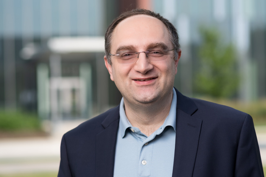
Purdue University Elmore Family School of Electrical and Computer Engineering professor Tillmann Kubis is calling for greater national attention to a critical but underrecognized skills gap in semiconductor education: quantum transport, the science of how electrons move through materials and devices when quantum mechanical effects become important.
Kubis says the issue is urgent because the semiconductor industry’s familiar technology node names, such as 5 nanometers or 2 nanometers, no longer mean what many people assume they mean. They are industry labels like product generation not literal measurements of the smallest features inside a chip, under an electron microscope a 5 nm transistor will typically have dimensions of 18 nm or 30 nm
That distinction matters, says Kubis. As semiconductor devices continue to shrink, electrons no longer behave in simple, classical ways. They can tunnel through barriers, scatter, act like waves and respond to materials in ways that require a deeper understanding of quantum mechanics. These effects can determine whether a future transistor, memory device or advanced computing system works as intended.
Quantum transport is already essential in advanced device engineering, semiconductor physics and research and development. It is used to understand tunneling, leakage currents, nanoscale transistor performance, novel materials, quantum devices and future technology nodes.
Kubis said the problem is not that the science is impossible. Purdue researchers, including Kubis, previously used atomistic quantum transport simulations to showcase nanowire transistors with gate lengths below 8 nanometers. That work showed that at such small dimensions, source-drain tunneling becomes a major performance-limiting factor and that quantum-aware engineering choices can improve device performance.
The bigger concern, Kubis said, is that too few students and engineers are being trained to understand and use this knowledge.
“This is a big risk and opportunity,” Kubis said. “The nation or company that has people who understand how to handle these quantum effects and make them work for transistors will have a very strong advantage.”
He said the shortage has become a circular problem. Students may not pursue quantum transport because they do not see many jobs explicitly asking for it. Companies may not advertise for the skill because the talent pool is too small. As a result, there is a risk expertise that could be essential for maintaining future semiconductor leadership is not developed and implemented in time.
The challenge also cannot be solved by artificial intelligence alone, Kubis said. AI can help sort through existing knowledge, but it cannot replace the deep physical understanding needed to model, test and design devices at true nanoscale dimensions.
Kubis is calling for a coordinated response across academia, industry and government. Universities should make quantum transport and advanced semiconductor physics more accessible to students and working engineers. Companies should invest in employees who can understand and use advanced simulation tools. Funding agencies and policymakers should recognize that semiconductor competitiveness depends not only on manufacturing capacity, but also on the people who understand the physics behind future devices.
The goal, Kubis said, is not to turn every engineer into a quantum mechanics expert. It is to make sure enough people across the semiconductor ecosystem have the training to ask the right questions, interpret advanced simulations and help guide the next generation of technology.
“Having no one know these physics concepts is a strong gamble that bets on competitors or adversaries to stay in the same situation,” Kubis said. “We better have some training, some educated users.”
For Kubis, the message is simple: The United States should not wait until the knowledge gap becomes a technology gap.
Future semiconductor leadership will require more than smaller node names. It will require deeper science, stronger training and a workforce ready to engineer devices at dimensions where quantum effects are no longer optional.