Abhijeet Paul

Orientation dependance of charge distribution in silicon nanowire transistors.

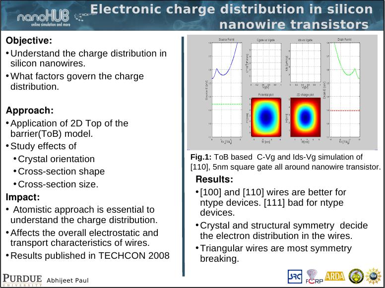
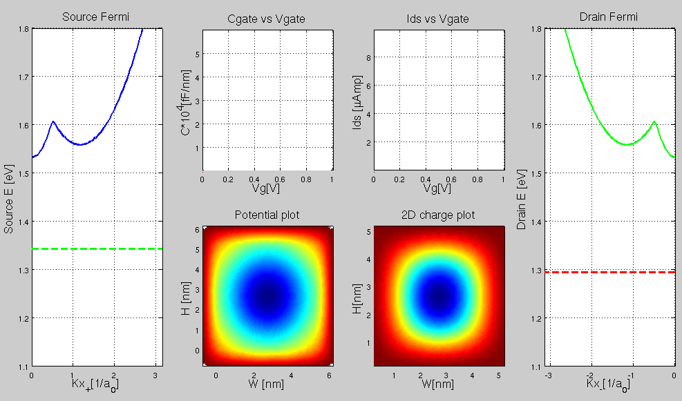
Electronic charge distribution in silicon nanowire transistors Abhijeet Paul, Neophytos Neophytou Mathieu Luisier and Gerhard Klimeck

Objective:

  • Understand the charge distribution in silicon nanowires.
  • What factors govern the charge distribution.

Approach:

  • Application of 2D Top of the barrier(ToB) model[J100]
  • Study effects of:
    • Crystal orientation
    • Cross-section shape
    • Cross-section size.

Impact:

  • Atomistic approach is essential to understand the charge distribution
  • Affects the overall electrostatics and transport characteristics of wires.
  • Results published in TECHCON 2008, [P96]

Results:

  • [100] and [110] wires are better for ntype devices. [111] bad for ntype devices.
  • Crystal and structural symmetry responsible the electron distribution in the wires.
  • Triangular wires are most symmetry breaking.

Powerpoint slide as ppt, pdf, or as image below.