Simulation and Optimization of an In-plane Thermal Conductivity Measurement Structure for Silicon Nanostructures
Simulation and Optimization of an In-plane Thermal Conductivity Measurement Structure for Silicon Nanostructures
Extended Abstract:
Thermal conductivity measurement of nanostructured materials have attracted significant attention in recent years due to their use in applications including thermoelectrics, thermal sensors, and MEMS actuators [1]. With low thermal conductivity and high electrical conductivity, Silicon nanostructures are expected to be promising thermoelectrics materials [2]. Several measurement structures using silicon-on-insulator (SOI) technology have been developed to measure the in-plane thermal conductivity of nanoporous silicon films [3]. Generally, suspended, steady-state measurement structures are used for measuring the in-plane thermal conductivity as the heat transfer is confined to the lateral direction.
Several groups have used these suspended measurement structures to measure in-plane thermal conductivity of different silicon nanostructures [4, 5]. However, few researchers have focused on the impact and optimization of important structural and measurement parameters such as heater and sensor geometry and current intensity. Numerical modeling allows optimization of these parameters prior to experimentation to ensure accurate measurement results. In this work, we first compare the coupled electro-thermal COMSOL simulations with existing experimental data for similar measurement structures. Then, we optimize the design of suspended steady-state joule heating measurement structures for porous nanostructured silicon materials to maximize the measurement accuracy for the range of expected sample thermal properties.
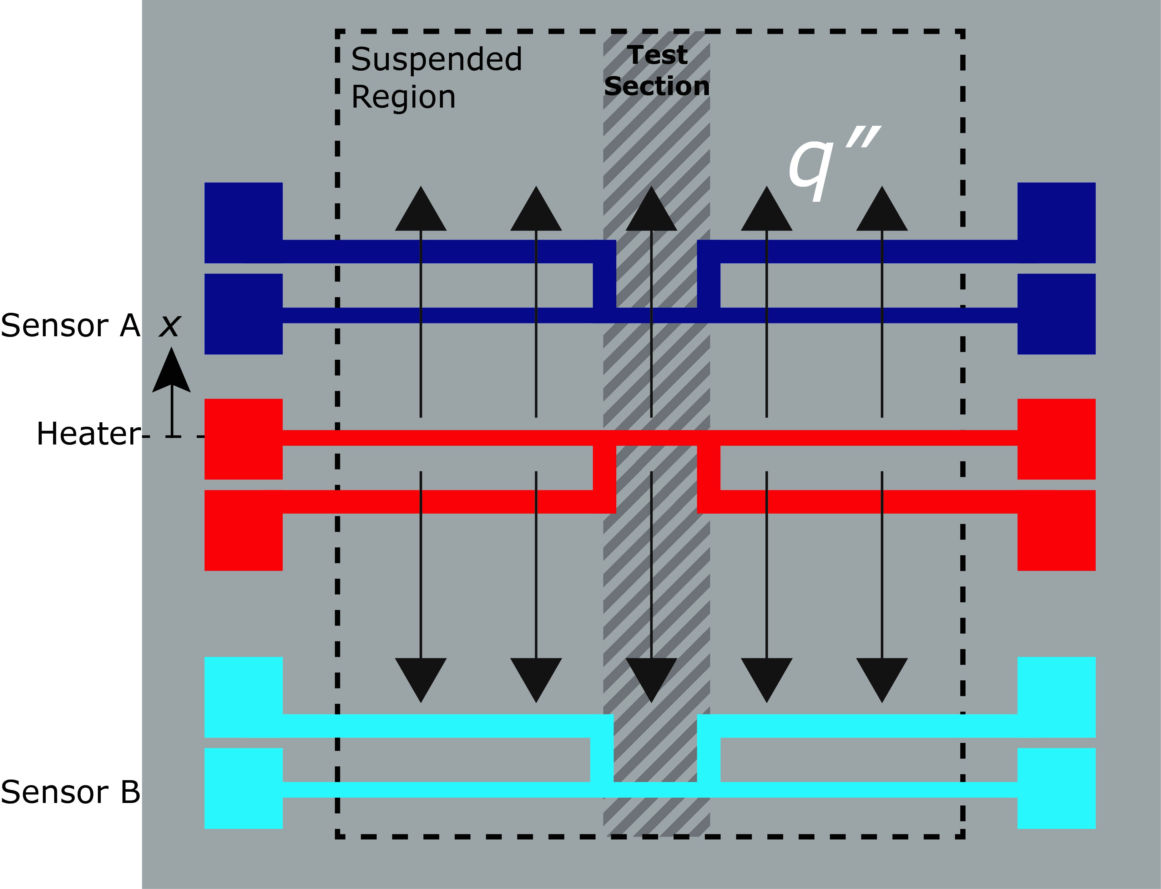 Figure 1: In-plane thermal conductivity measurement structure for silicon nanostructures. One heater and two sensor resistive metal lines are patterned on the suspended sample region to measure the thermal properties. Current flowing through the center heater line generates a known heat flux, which is conducted to the edges of the sample region. In the test section (e.g. the center portion of the suspended region), the heat flow is generally one-dimensional and the in-plane thermal conductivity can be determined by measuring the temperature at two positions from the heater line as a function of input heater power.
In this work, we focus on silicon nanostructures fabricated from SOI wafers as shown in Figure 1. Heat generated at the center metal heater line is conducted across the thin film to the unsuspended portions of the sample, which act as heat sinks. The heat flow is nearly one-dimensional in the test section near the center of the heater line. Two additional metal lines are used as resistive thermometers to measure the resulting temperature profile as a function of input heater power. For both the heater and sensor lines, voltage probes are connected near the center of the metal lines to measure the resistance of the test section only, which is dependent on the temperature of the metal lines.
In this work, we investigate the impact of measurement geometry and conditions on the accuracy of the thermal property measurements. Specifically, we examine the impact of the heater and temperature sensor design, current input intensity, and relevant heat loss issues using a coupled electro-thermal COMSOL model of the experimental structure. By varying the device geometry, heater and sensor currents, and expected thermal conductivity of the test section, simulated experimental data is obtained which is then analyzed with a one-dimensional, steady state heat transfer model. The placement of the sensors and the separation of the voltage probes are critical to ensuring that heat transfer is one-dimensional in the test section. Furthermore, the temperature rise of the heater line must be small to minimize radiative heat losses, but large enough for accurate temperature measurements at the sensor lines. Beyond the thermal transport considerations, limitations of the fabrication process and mechanical strength of the suspended region must be considered.
In summary, we optimize a suspended structure for measuring the in-plane thermal conductivity of nanoporous silicon and silicon nanowire arrays using an electro-thermal transport model. Improved measurement structures will yield more accurate thermal conductivity results for these complex nanostructures, which will shed light on phonon transport mechanisms [7, 8].
References
1. A. D. McConnell and K. E. Goodson, Thermal Conduction in Silicon Micro- and Nanostructures. pp. 129–168.
2. T. Kodama, A. Marconnet, J. Lee, M. Asheghi, and K. E. Goodson, “In-plane thermal conductivity measurement on nanoscale conductive materials with on-substrate device configuration,” 13th Intersoc. Conf. Therm. Thermomechanical Phenom. Electron. Syst., pp. 250–255, May 2012.
3. A. M. Marconnet, T. Kodama, M. Asheghi, and K. E. Goodson, “Phonon Conduction in Periodically Porous Silicon Nanobridges,” Nanoscale Microscale Thermophys. Eng., vol. 16, no. 4, pp. 199–219, Dec. 2012.
4. D. Song and G. Chen, “Thermal conductivity of periodic microporous silicon films,” Appl. Phys. Lett., vol. 84, no. 5, p. 687, 2004.
5. M. Asheghi, K. Kurabayashi, R. Kasnavi, and K. E. Goodson, “Thermal conduction in doped single-crystal silicon films,” J. Appl. Phys., vol. 91, no. 8, p. 5079, 2002.
6. S. R. Mirmira and L. S. Fletcher, “Review of the Thermal Conductivity of Thin Films,” J. Thermophys. Heat Transf., vol. 12, no. 2, pp. 121–131, Apr. 1998.
7. D. G. Cahill, W. K. Ford, K. E. Goodson, G. D. Mahan, A. Majumdar, H. J. Maris, R. Merlin, and S. R. Phillpot, “Nanoscale thermal transport,” J. Appl. Phys., vol. 93, no. 2, p. 793, 2003.
8. W. Liu and M. Asheghi, “Phonon–boundary scattering in ultrathin single-crystal silicon layers,”