From the Casimir Limit to Phononic Crystals: Twenty Years of Phonon Transport Studies using Silicon-on-Insulator Technology
From the Casimir Limit to Phononic Crystals: Twenty Years of Phonon Transport Studies using Silicon-on-Insulator Technology
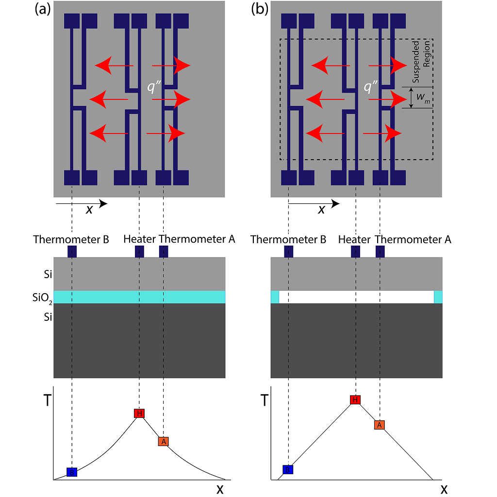
Silicon-on-insulator (SOI) technology has sparked advances in semiconductor and MEMs manufacturing and revolutionized our ability to study phonon transport phenomena by providing single-crystal silicon layers with thickness down to a few tens of nanometers. These nearly perfect crystalline silicon layers are an ideal platform for studying ballistic phonon transport and the coupling of boundary scattering with other mechanisms, including impurities and periodic pores. Early studies showed clear evidence of the size effect on thermal conduction due to phonon boundary scattering in films down to 20 nm thick and provided the first compelling room temperature evidence for the Casimir limit at room temperature. More recent studies on ultrathin films and periodically porous thin films are exploring the possibility of phonon dispersion modifications in confined geometries and porous films.