Electrically Induced Directional Ion Migration in Two-Dimensional Perovskite Heterostructures
Electrically Induced Directional Ion Migration in Two-Dimensional Perovskite Heterostructures
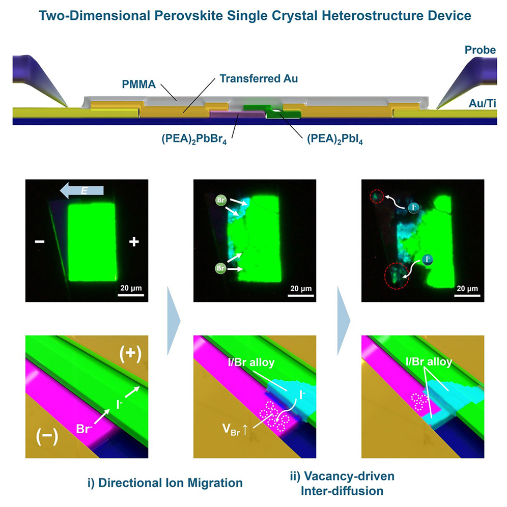
Understanding ion migration in two-dimensional (2D) perovskite materials is key to enhancing halide perovskite device performance and stability. However, prior studies have been primarily limited to heat and light induced ion migration. In this work, to investigate electrically induced ion migration in 2D perovskites, we construct a high-quality single crystal 2D perovskite heterostructure device platform with near defect-free van der Waals contact. While achieving real-time visualization of halide anions migrating towards the positive bias, defined here as directional ion migration, we also uncover the unique behavior of halide anions inter-diffusing towards the opposite direction under prolonged bias. Confocal microscopy imaging reveals a halide migration channel that aligns with the crystal and heterojunction edges. After a sustained ion migration, stable junction diodes exhibiting up to ~1000-fold forward to reverse current ratio are realized. This study unveils important fundamental insights on halide migration under electrical bias, paving the way towards high-performance devices.