Welcome to Professor Michael D. Sangid's research webpage for the Advanced Computational Materials and Experimental Evaluation (ACME2) Laboratory in the School of Aeronautics and Astronautics at Purdue University. Research in the ACME2 lab combines knowledge of materials science, solid mechanics, and advanced manufacturing to solve complex problems in the mechanical behavior and processing of aerospace structural materials.
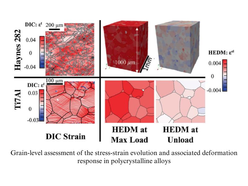
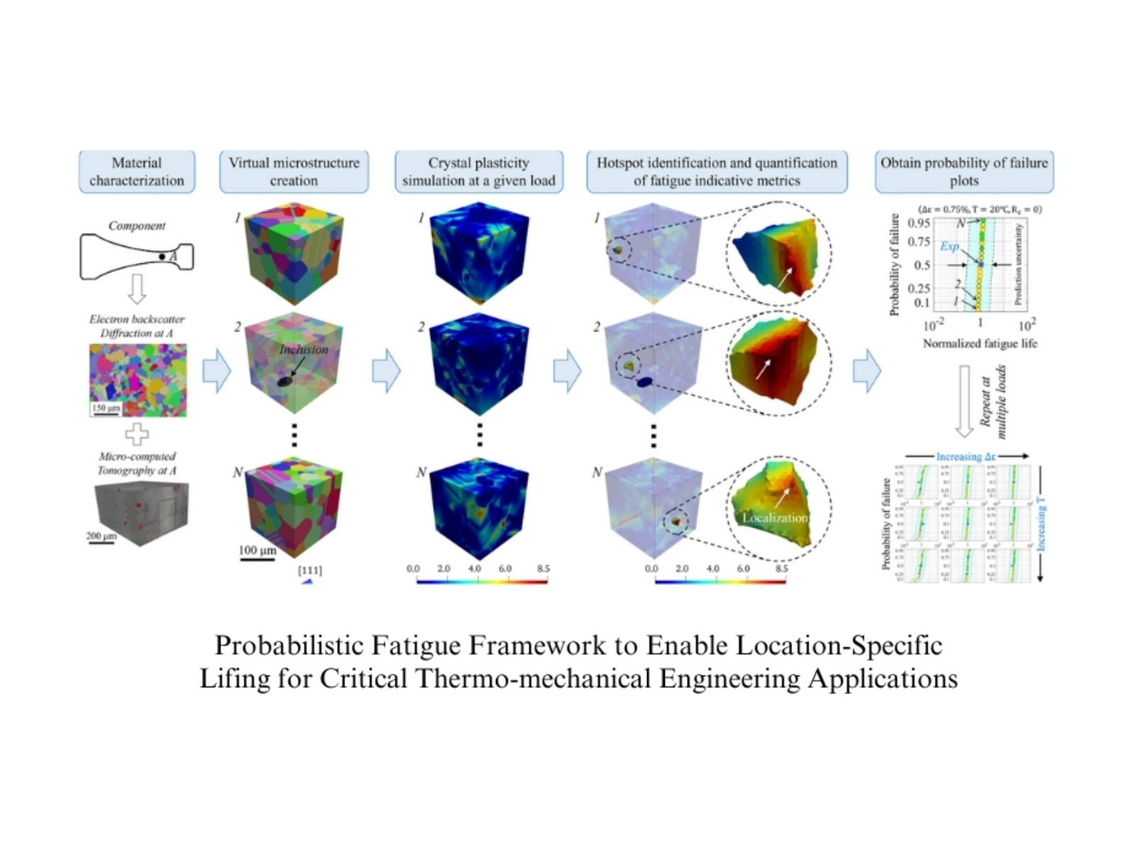
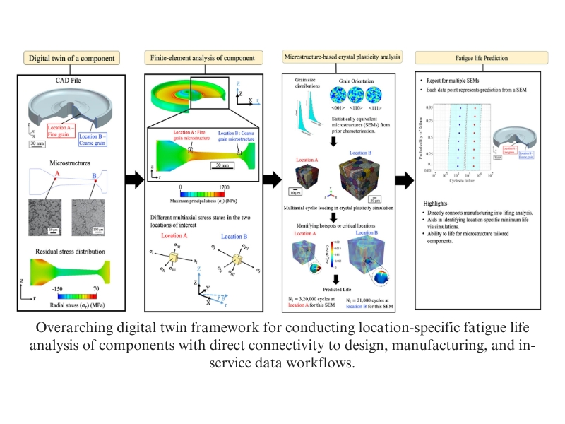
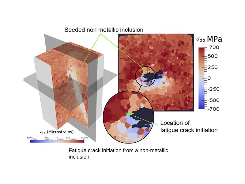
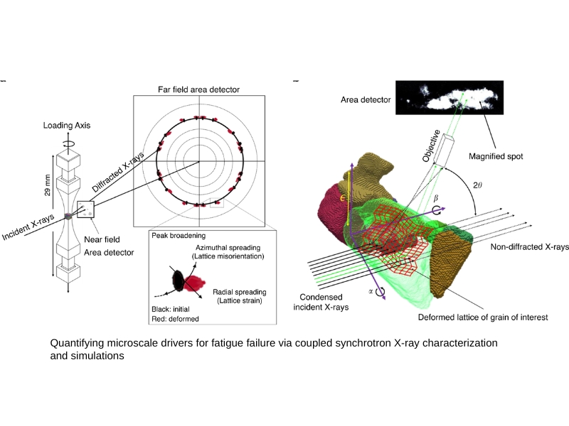
In our research, we employ physics-based computational modeling and design tools, which are experimentally validated and verified. We aim to improve our understanding and our tools for designing, processing, and lifing materials through simulation-based modeling of the material’s microstructure and defects. Many times, it is necessary to start at the defect and microstructural level (e.g. the meso-scale) to gain a quantifiable understanding of the deformation and failure mechanisms at component scales, while exercising the most advanced characterization and interrogation methods at each scale to verify and validate predictions of the simulations, including electron microscopy and synchrotron-based X-ray imaging to map the evolution of the stress/stain state or microstructure/defect features during applied thermo-mechanical loading. The ACME2 group simultaneously addresses fundamental research needs and implements this knowledge into an integrated model that can directly aid in and transform the design methodology providing pragmatic engineering solutions. The uniqueness of our modeling approach is that it avoids large-scale empirical testing programs and the requirement to locking-down the processing route of materials prevalent in classical engineering models, while providing a general framework, which allows:
(1) Easy integration and modification of software,
(2) Ability to modify process route or component geometric design to achieve targeted and improved material properties,
(3) Uncertainty quantification and probabilistic lifing, and
(4) Pragmatic tools to answer production questions or rapidly qualify new materials and processes.
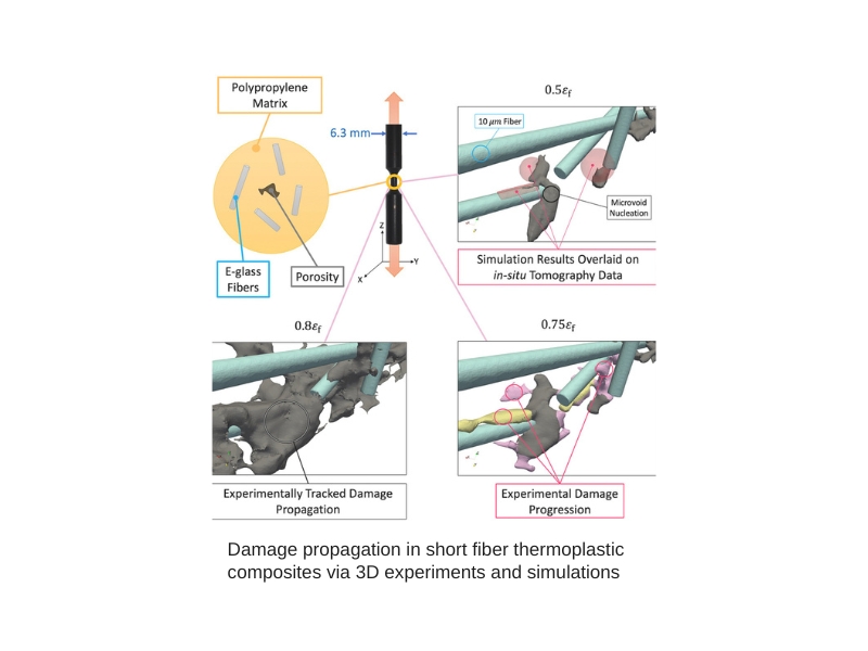
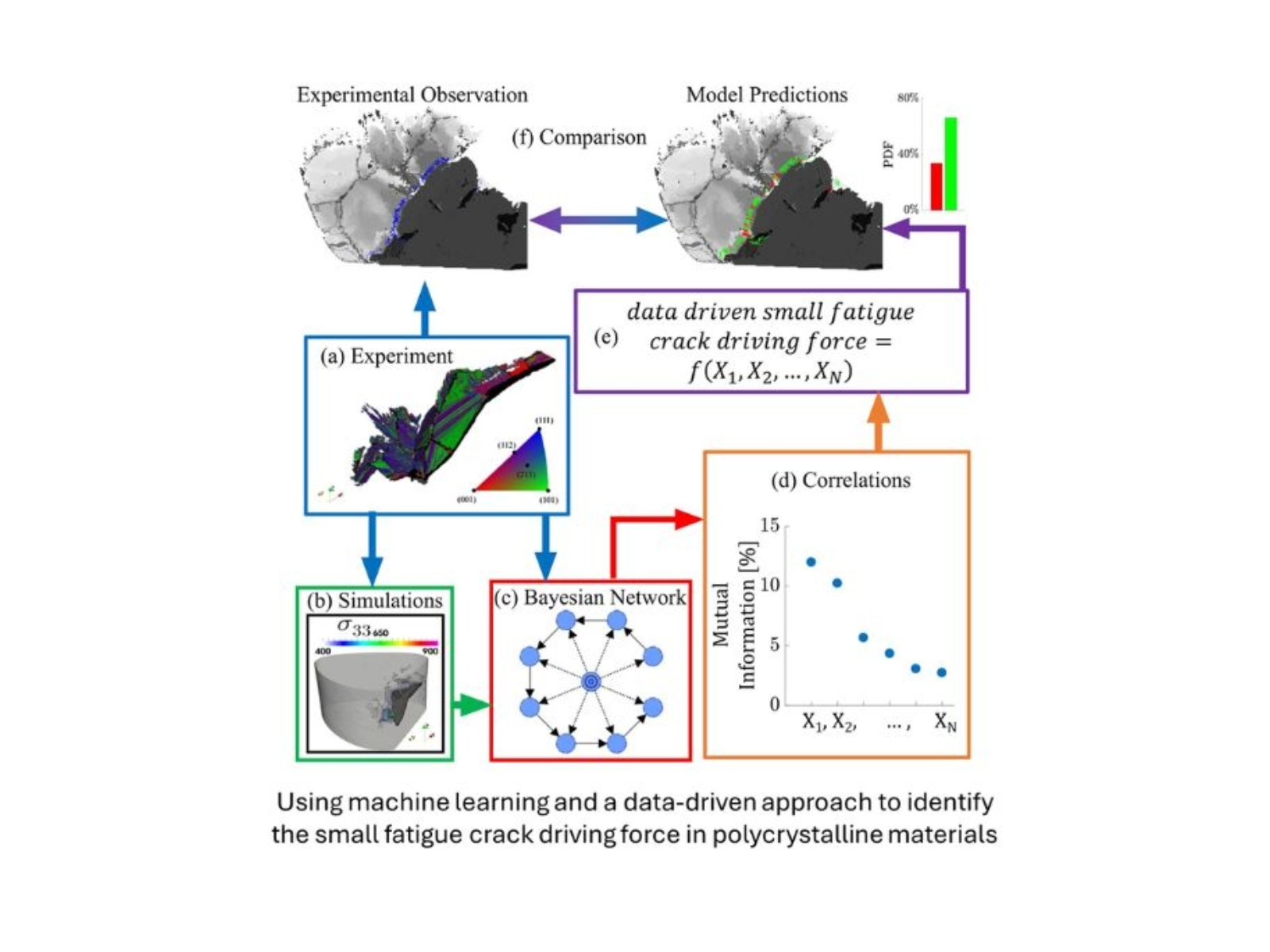
Thus, the ACME2 group combines computational modeling and simulations, advanced characterization, data driven approaches, in situ experiments, and coupon-scale testing to solve theoretical and complex applied problems in Aerospace materials. Aerospace structural materials of interest include high temperature engineering alloys, lightweight alloys, fiber reinforced polymer composites, ceramic matrix composites, and carbon-carbon composites.
For more information including an extended CV, please email Prof. Michael D. Sangid.
In this website you will find an overview of ACME2 current projects and facilities, as well as information about our group members. Finally, in Greek, ACME (ακμή) denotes the peak, zenith, prime, or best and we will continually strive to live up to the quality of research.

