UPWARDS NETWORK
A US JAPAN Collaboration for Semiconductor Workforce Development
Overview

Purdue President Mung Chiang signed a landmark international agreement on May 21, 2023, at the G7 Summit in Hiroshima, Japan, partnering with Micron, Tokyo Electron (TEL) and other educational institutions in the United States and Japan to establish the "UPWARDS Network" for workforce advancement and research and development in semiconductors. This partnership cultivates a more diverse, robust and highly skilled talent pipeline for the semiconductor workforce and drives emerging research while increasing the pipeline of students studying a semiconductor curriculum.
Micron and TEL, the National Science Foundation (NSF) and the universities are expected to invest more than $60 million in the network. These funds will support the launch and implementation of this innovative network, which deepens ties between industry and higher education across the U.S. and Japan. The network is expected to impact approximately 5,000 students per year.
The semiconductor industry requires a highly skilled and diverse workforce that can strengthen technology leadership and innovation across ecosystems in the U.S. and Japan. Partnerships between universities and companies are critical to developing semiconductor talent, cross-collaboration and expanding cutting-edge research.
The Focus
- Develop the next generation of the workforce, enabling fundamental and emerging research, with a priority to expand opportunities to female students, researchers and leaders.
- Develop leading semiconductor curricula and creating opportunities for cross-collaboration.
- Provide access to experiential learning in cleanrooms and memory-related research across institutions, with a particular focus on promoting opportunities for female students, staff and leaders.
- Students from all 11 universities will have the opportunity to study at partner institutions and will be encouraged to apply for internships and full-time positions at Micron and TEL.
The 5 Core Pillars

A set of courses have been developed and recorded. They are Introduction to "Data Analytics, Design of Experiments, and Machine Learning" and "Reliability Physics of Advanced Packaging." A new VR-based module for memory fabrication is being developed (see the following section for more detail).
The UPWARDS Purdue team had an open call for proposals on curriculum development and experiential learning in May, 2024. The following two projects were selected, and they are being developed.
-
Project Title: Emerge: Exploring Memory Education via
Realistic Generated Experiences
PIs: Prof. Mustafa Hussain and Prof. Dimitrios Peroulis - Purdue ECE
vFabLab is an innovative virtual platform providing in-depth, interactive training on semiconductor device fabrication. Accessible worldwide, it has trained over 1,700 students from 540+ institutions, effectively preparing them for cleanroom operations. This project aims to enhance vFabLab by integrating 3D headset compatibility and offering specialized training on memory device fabrication, including SRAM, DRAM, and non-volatile memory. The platform?s objectives include democratizing access to high-quality semiconductor education and fostering a global community for collaboration and lifelong learning. The objectives are multifaceted: 1. Comprehensive Training: Deliver in-depth training modules covering the fabrication processes of diverse memory devices. 2. Skill Enhancement: Provide practical experience in memory device fabrication through virtual simulations. 3. Specialized Focus: Tailor training modules to address the specific intricacies of different memory device types. 4. Global Accessibility: Make vFabLab accessible worldwide, democratizing access to high-quality training resources. 5. Continuous Improvement: Enhance vFabLab's capabilities based on user feedback and industry advancements.
-
Project Title: 2D-FeFET Embedded DRAM for On-Chip DNN
Training with Floating-Point Compute-In-Memory Design
PIs: Prof. Haitong Li (Purdue), Prof. Joerg Appenzeller (Purdue), Prof. Akinobu Teramoto (Hiroshima University), Prof. Haruka Suzuki (Nagoya University), Prof. Zhihong Chen (Purdue)
The team proposes a co-designed 2D-material ferroelectric FET (2D-FeFET) based embedded DRAM (eDRAM) solution for memory-centric AI hardware, specifically for on-chip DNN training with floating-point precisions. Utilizing transition metal dichalcogenides (TMDs) as high-performance channels and a ferroelectric gate stack in a 2-T gain-cell structure, we aim to achieve scalable CIM operations. This project covers material characterization, memory-centric computing, and experiential learning. The proposed design promises significant energy savings compared to advanced CMOS accelerators, with plans for hands-on student training and international collaboration. In Experiential Learning thrust, specifically, based on the proposed co-design drivers, the team will launch a new course project in the Purdue VIP course, Semiconductors@ Birck, providing hands-on nanofabrication and characterization experience to undergraduate students. A Purdue-Hiroshima-Nagoya joint workshop will also be held, and student exchange visits will be organized.
Purdue will fund four Ei-ichi Negishi fellowships, to further develop curriculum and R&D; in areas of interest to the UPWARDS program. (Dr. Negishi: Japanese-American, Purdue faculty, 2010 Nobel Prize recipient in Chemistry).
The UPWARDS program has appointed 12 women faculty (UPWARDS faculty), promoting research opportunities, diversity and nurturing future talent. It has also reached 780 female students through events and classes, such as "Inclusive Society" and "My Dream for Engineering".
-
Appointment of UPWARDS Faculty
Dan Jiao was selected as Purdue's UPWARDS PI (Industry). She is the Synopsys Professor in Purdue University's Elmore Family School of Electrical and Computer Engineering. She directs Rapid-HI (Heterogeneous Integration) Design Institute, an Elmore ECE Emerging Frontiers Center. A fellow of the IEEE and a Distinguished Microwave Lecturer of the IEEE MTT Society, Jiao has authored over 350 papers in refereed journals and international conferences. Her research has been recognized by the 2022 Computational Electromagnetics Award of the ACES society, the 2019 Intel's Outstanding Researcher Award, the 2013 Sergei A. Schelkunoff Prize Paper Award of the IEEE Antennas and Propagation Society (AP-S), numerous Best Paper Awards and Finalists in conferences. She was one of 85 selected for the National Academy of Engineering's (NAE) 2011 U.S. Frontiers of Engineering Symposium, a recipient of the NSF Career Award in 2008, the Intel Logic Technology Development Divisional Achievement Award in 2003, and the 2000 Raj Mittra Outstanding Research Award. She has been appointed the editor-in-chief of the IEEE Journal on Multiscale and Multiphysics Computational Techniques.
-
Summer camp for women.
Tokyo Electron organized an exciting summer program: "UPWARDS Summer Camp for Women".
This is a program for female students at universities participating in UPWARDS. "Staying at 'Tokyo Electron Karuizawa Club' in Nagano, students can learn about everything from semiconductors to Tokyo Electron while enjoying some fun activities!"
-
Held: Aug 20 through Aug 22
Enrollment: 1 to 3 students per university
More information about this program (Japanese & English)
-
-
Women researchers and students in semiconductors.
Prof. Shubhra Bansal's research project titled "Electro- and Thermo-migration Analysis of Cu-pillar Assembly at sub-10 micron Pitch" has been selected for funding by Purdue's UPWARDS program. Three female students have also been recruited into the UPWARDS research program.
Our "Semiconductors in Japan" study abroad program held from May 5 to May 18 in Japan has 18% female students.
The experiential learning has been integrated into multiple other pillars of the UPWARDS program.
Integration with Pillar 5 (exchange program): In Hiroshima University's visit to Purdue from Feb. 24 to March 5, 2024, students visited Purdue's Birck Nanotechnology Center, attended technical lectures, participated in CHIPS seminar with ~100 students, and visited local companies and cultural events. In Purdue students' visit to Japan in May 2024, students visited the Center for Innovative Integrated Electronic Systems (CIES) at Tohuku University and listened to lectures related to semiconductors.
Integration with Pillar 4 and Pillar 1 (research and curriculum program): Undergraduate and graduate students are involved in the four research and education programs funded by UPWARDS. They have gained hands-on experiences and received comprehensive training on various memory device fabrication processes, including SRAM, DRAM, and non-volatile memory.
Purdue hosted three faculty-led workshops for the faculty from Hiroshima and Tohoku universities. This allowed the groups to harmonize research and teaching plans.
The UPWARDS Purdue team had an open call for proposals on collaborative research in May, 2024. The following three research projects were selected.
-
Project Title: Full 3D thermal map reconstruction of commercial processing-in-memory 3D stacks
PIs: Prof. Peter Bermel (Purdue), Prof. Seiichiro Higashi (Hiroshima University), David Guzman (Micron Technology)
This project explores the potential of Processing-in-Memory (PIM) technologies using 3D stacks like high-bandwidth memory (HBM) to enhance performance by reducing power consumption and latency. The increased thermal load from PIM poses significant thermal management challenges, which this research addresses through advanced thermometry and thermo reflectance imaging techniques. By combining experimental data with 3D thermal modeling, the project aims to create a detailed thermal map of a PIM/HBM stack, identifying hot spots and failure risks. Additionally, it supports workforce development through a new course and industry internships for students.
Publication. Lee, Changkyun, Jiawei Song, Haiyan Wang, Jie Zhu, Vidisha Singhal, and Peter Bermel. "Temperature-dependent optical dispersion of composite oxide multilayers." In Nonimaging Optics: Efficient Design for Illumination and Concentration XIX, p. PC1313207. SPIE, 2024.
-
Project Title: Electro- and Thermo-migration Analysis of Cu-pillar Assembly at sub-10 micron Pitch
PI: Prof. Shubhra Bansal (Purdue)
This project focuses on advancing Cu-pillar hybrid bonding technology to meet the demands of high-performance memory and computing, particularly for the 1 nm Silicon Node. The research evaluates the thermo-migration and electromigration reliability of Cu-pillar thermo-compression bonding with low-temperature solder for chip-to-package interconnections at a 5 �m bump pitch. The study combines modeling and experimental approaches to assess bond strength, void formation, and electromigration resistance. Additionally, it supports the development of a 9-credit concentration in Heterogeneous Integration & Advanced Packaging as part of the DOD SCALE program.
-
Project Title: 2D-FeFET Embedded DRAM for On-Chip DNN Training with Floating-Point Compute-In-Memory Design
PIs: Prof. Haitong Li (Purdue), Prof. Joerg Appenzeller (Purdue), Prof. Akinobu Teramoto (Hiroshima University), Prof. Haruka Suzuki (Nagoya University), Prof. Zhihong Chen (Purdue)
Emerging memory-intensive applications, including the secure fine-tuning of large language models for downstream tasks in edge devices (autonomous vehicles, robots, AR/VR), are steering the advancement of memory-centric AI hardware towards on-chip DNN training with floating-point precisions. Incumbent memory technologies and inference accelerators fall short of meeting these demands. The team proposes a co-designed 2D-material ferroelectric FET (2D-FeFET) based embedded DRAM (eDRAM) solution for memory-centric AI hardware, specifically for on-chip DNN training with floating-point precisions. Utilizing transition metal dichalcogenides (TMDs) as high-performance channels and a ferroelectric gate stack in a 2-T gain-cell structure, the team aim to achieve scalable CIM operations. This project covers material characterization, memory-centric computing, and experiential learning. In Material Characterization thrust, experimental 2D-TMD material characterizations will be performed with ferroelectric gate stacks and fabricate/optimize 2-T eDRAM primitives employing 2D-FeFETs. Key technology specs of the hybrid eDRAM will be characterized for benchmarking. In Memory-Centric Computing thrust, the team will experimentally demonstrate precision-scalable CIM operations on the developed platform, with 2 x 2 array prototypes to be fabricated. Calibrated with electrical measurements, an architecture simulator with CIM circuits will be built to enable cross-layer design space explorations for FP-training and INT-inference. To collectively identify future optimizations, Dr. Teramoto (Hiroshima Univ) will conduct surface analysis (XPS/XRD/AFM) using Purdue's devices, and Dr. Suzuki (Nagoya Univ) will explore plasma etching/deposition.
- Publication: L. Zheng and H. Li, "CMOS+X Technologies for Neuro-Vector-Symbolic Computing," Device Research Conference (DRC), June 2024.
- Dr. Li organized a special session at ICCAD 2024 on edge AI and role of emerging memories
- Dr. Li gave an invited talk at ESWEEK 2024 on memory-centric computing.
-
First Japanese partner visit: Hiroshima University visit to Purdue, Feb. 24 - Mar. 5, 2024.
Purdue hosted a short-term academic visit for nine diverse Hiroshima University students led by Ms. Kaori Taka, Chief of Global Initiatives Group, International Office at Hiroshima University and Dr. Taiji Hotta, Vice-Executive Director of Super Global University (SGU) Project, Director of the Office of Global Initiative, Hiroshima University, and Professor, Center for the Study of International Cooperation in Education (CICE), the IDEC Institute. The visit program incorporated lab visits, technical lectures, local company visits (e.g., Subaru) and cultural visits.
Hiroshima University welcome reception was held on Feb. 26, 2024 (see photo below), where Hiroshima students and program leaders met with Purdue leadership and student mentors during their first day of campus activities.

-
Purdue UPWARDS Study Abroad program, "Semiconductors in Japan," held May 5 to May 18, 2024.
The program was led by Purdue University's Vice President Cristina Farmus and George Chiu, assistant dean for Global Engineering Programs and professor of mechanical engineering. Twenty-two Purdue undergraduate students visited Japan to learn more about the semiconductor industry and technical advancements. They visited universities and companies that are part of the UPWARDS network, including Tokyo University, Tohoku University, Hiroshima University, Tokyo Electron Company and Micron, among other relevant visits. They also listened to lectures related to semiconductors.
Visit the following link for more info:
https://web.tohoku.ac.jp/ged/12430?lang=en


-
Purdue First-Year-Engineering study abroad program "Global Design and Practice for Pre-engineering in Taiwan and Japan."
Participants visited Japan from June 15-30, 2024. They visited world-class semiconductor companies as well as UPWARDS university partners, like Tohoku University. The program has yielded 40% female participation historically.

As a world class university that moves fast and gets things done, Purdue pursues excellence at scale, with the largest engineering college (over 16,000 engineering students) ever ranked among the top 4 in the U.S.
UPWARDS Faculty

Muhammad Ashraful Alam
Principal Investigator
National Science Foundation
Jai N. Gupta Distinguished Professor of Electrical and Computer Engineering
View Profile
Dan Jiao
Principal Investigator (Industry)
Synopsys Professor of Electrical and Computer Engineering
View Profile
David B. Janes
Professor of Electrical and Computer Engineering
Director
of Project Track Master's Program

Mark Lundstrom
Don and Carol Scifres Distinguished Professor of Electrical and
Computer Engineering
Purdue Chief Semiconductor Officer

Vijay Raghunathan
Vice President for Global Partnerships and Programs
Director
of Semiconductor Education
Professor of Electrical and
Computer Engineering
News Stories
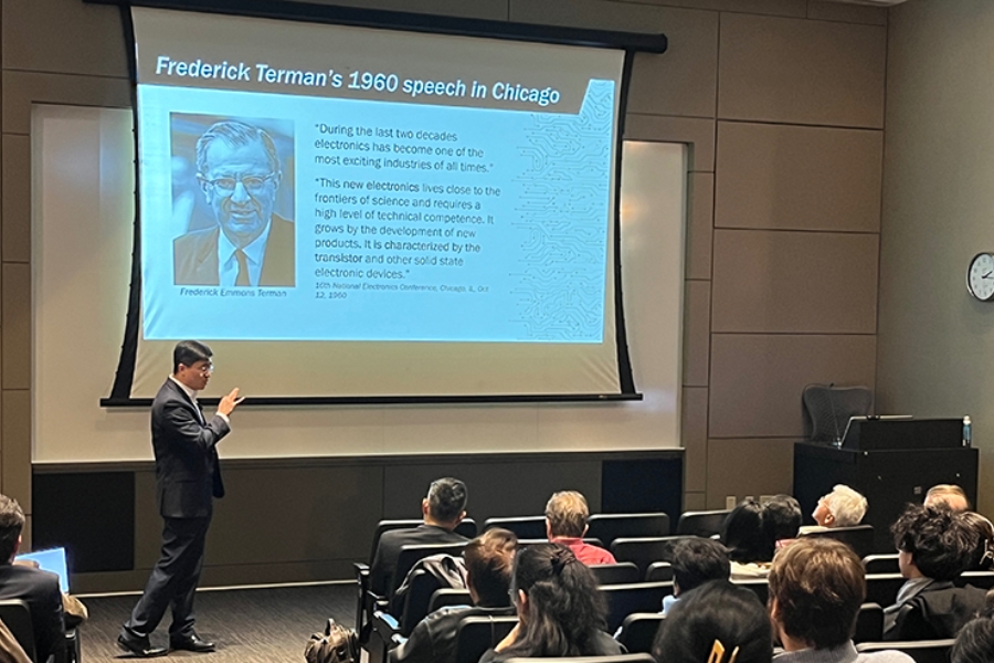
Chiang provides keynote lecture on CHIPS at Columbia University
October 25, 2024
On Oct. 17, Purdue President Mung Chiang delivered the Armstrong Memorial Lecture for the Columbia University Electrical Engineering Department titled “CHIPS: Execute for Success.” He explained Purdue’s initiatives related to semiconductor innovation and discussed the role of research universities in talent development, research moonshots and public private partnership. Chiang’s presentation was co-authored by Mark Lundstrom, chief semiconductor officer for Purdue.
Read Full Article
Purdue Semiconductor Degrees
October 23, 2024
Purdue's comprehensive new Semiconductor Degrees Program (SDP) is a suite of innovative credentials and degrees that will educate both graduate and undergraduate students, enabling a quick ramp-up of skilled talent and creating the next-generation of semiconductor workforce to reassert American preeminence in this critical industry.
Read Full Article
Why earning a semiconductor certification is a game-changer
October 23, 2024
A first-hand student account of a two-week study abroad program in Japan.
Read Full Article
Two years since the CHIPS Act, the race heats up to train tens of thousands of workers
August 9, 2024
President Joe Biden signed the CHIPS and Science Act into law on Aug. 9, 2022, authorizing nearly $53 billion to rebuild the nation’s semiconductor industry. With chip factories breaking ground from Syracuse, New York, to Phoenix in the two years since, the focus has grown on how to fill them with the next generation of workers — like Robert Zhang.
Read Full Article
U.S. Department of Commerce Announces Preliminary Terms with SK hynix to Advance U.S. AI Supply Chain Security
August 6, 2024
Biden-Harris Administration’s Bipartisan CHIPS and Science Act Attracts All Five Major Leading-Edge Logic and Memory Companies to Produce Chips on U.S. Soil
Read Full Article
Purdue and leading microelectronics industry association SEMI partner to bolster semiconductor education
June 26, 2024
Purdue University is partnering with SEMI, the leading global microelectronics industry association, to create online courses aimed at bolstering the semiconductor workforce.
Read Full Article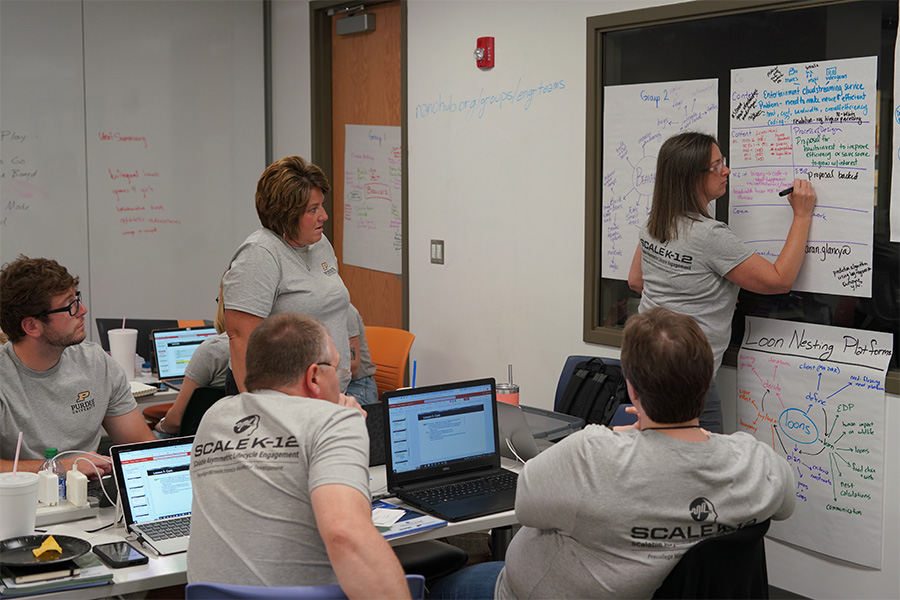
Purdue, DOD collaboration to embed microelectronics learning in Indiana classrooms expands to adjacent states
April 2, 2024
Select schools from Illinois and Michigan will join a growing number of Indiana school districts participating in a Purdue University-led program to embed microelectronics in K-12 classrooms as part of a DOD strategy to build a domestic semiconductor industry. Led by ENE's Tamara Moore, SCALE K-12 was awarded $2.5M from the Silicon Crossroads Microelectronics Commons Hub to expand its reach.
Read Full Article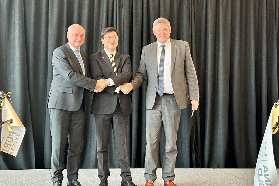
Imec expands its presence in the USA
December 8, 2023
Imec – a world leader in semiconductor R&D – is joining forces with Purdue University for R&D on novel semiconductor materials, systems, and sustainable manufacturing and has a Memorandum of Understanding (MOU) with the University of Michigan to jointly advance semiconductor technologies for the automotive industry. As part of the collaboration agreements, imec will set up a physical presence in both locations to support smooth collaboration and enriched knowledge sharing – to the benefit of all parties.
Read Full Article
Chipshub: An online platform for everything semiconductors
November 9, 2023
Purdue University is leveraging its expertise in scientific simulation tools to help the nation take the lead as the hub for semiconductors and chips research, development and manufacturing. The university is teaming with the state of Indiana, the U.S. Department of Defense and the international not-for-profit R&D center imec to unveil Chipshub, an online platform for semiconductor simulations, software, collaboration and workforce development.
Read Full Article
U.S. needs to invest in training, recruiting to expand semiconductor workforce
August 25, 2023
Chipmaker Nvidia reported this week that it doubled its quarterly revenue from a year ago. Its dominance in semiconductors for artificial intelligence is based on products that are manufactured overseas.
Read Full Article
Seeing STARS: Purdue trains next generation of semiconductor engineers
August 24, 2023
As their campus tour wound its way through Purdue’s Birck Nanotechnology Center, Raygan Bingham and her mom peered through the windows of the facility’s semiconductor cleanroom.
Read Full Article
The Economist: America is building chip factories. Purdue leading the charge to find the workers.
August 5, 2023
Judged by one measure, America’s new industrial policy is off to a roaring start. Enticed by subsidies, companies are pouring money into semiconductor plants and electric-vehicle factories. With investment in manufacturing facilities running at a record high, President Joe Biden’s claim that the future will again be “made in America” seems more credible than it once did.
Read Full Article
Summer program helps students develop skills for growing semiconductors industry
June 27, 2023
Devin Singh always has been interested in chips. He’d worked on some personal projects in the past making emulators for consoles like Nintendo Game Boy and Game Boy Advance, and he was interested in the process of combining simple components into making a functional machine that could do “cool things,” like play video games.
Read Full Article
Purdue, TSMC extend partnership on semiconductor research and workforce development
June 22, 2023
Purdue University continues to advance semiconductor workforce development by renewing a strong partnership between industry leader Taiwan Semiconductor Manufacturing Co. and the university’s Center for Secure Microelectronics Ecosystem.
Read Full Article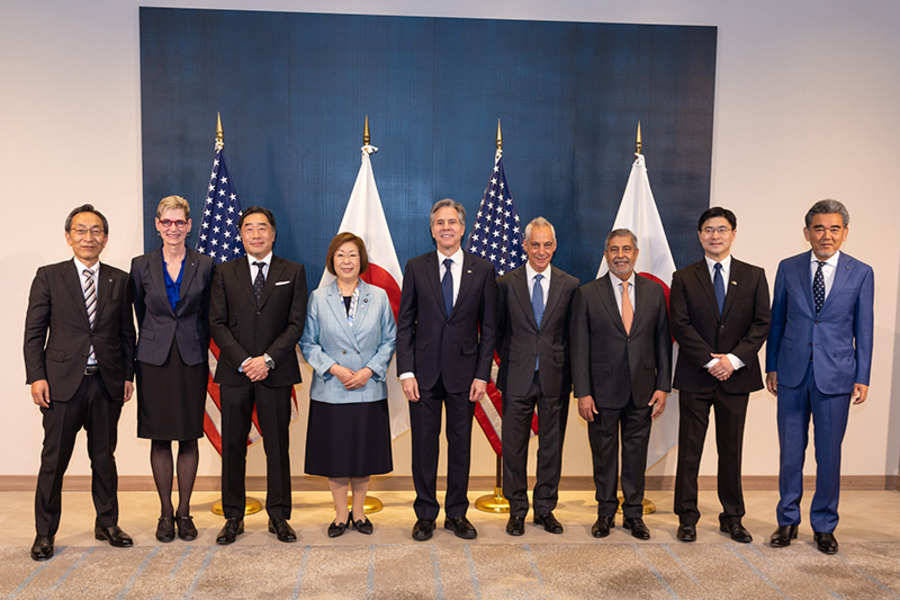
Purdue signs landmark U.S.-Japan agreement in semiconductors at G7 summit
May 22, 2023
Purdue University continues to be the world leader in creating vital partnerships in semiconductors. On Sunday (May 21) in Hiroshima, Japan, Purdue President Mung Chiang signed another landmark international agreement, partnering with Micron, Tokyo Electron and other educational institutions in the United States and Japan to establish the "UPWARDS Network" for workforce advancement and research and development in semiconductors.
Read Full Article
This university is addressing the shortage of U.S. semiconductor engineers
March 2, 2023
Purdue University is No. 16 on Fast Company’s list of the World’s 50 Most Innovative Companies of 2023. Explore the full list of companies that are reshaping industries and culture.
Read Full ArticleResearch Funded Projects
Shubhra Bansal, Principal Investigator
Associate Professor of Mechanical Engineering and Materials Engineering
As the demand for high performance computing increases, interconnect and die attach materials are needed to meet the requirements of 0.5 �m line width, sub-10 �m bump pitch, high I/O density, and power density for 1 nm Silicon Node and beyond. Cu-pillar technology with hybrid bonding has achieved sub-5 �m bump pitch posing several benefits such as increased I/O density, increased bandwidth, improved 3D stacking, enhanced power efficiency, and reduced parasitics and thermal resistance attributed to the absence of underfill. Although wafer-to-wafer (W2W) hybrid bonding can achieve 50 nm alignment accuracy; thermal budget, reliability, and chip-to-substrate hybrid bonding remain as drawbacks of this technology. In this study, thermo-migration, and electromigration reliability of Cu-pillar thermo-compression bonding via low-temperature solder will be evaluated for chip-to-package interconnections at 5 �m bump pitch. Reliability will be evaluated using combined modeling and characterization approach for thermo-mechanical and electromigration failures for Cu-In, Cu-Sn-Ag and Cu-Sn-Bi material systems through test structure evaluations. Daisy chain Cu- pillars with sub-10 �m pitch and planar serpentine test structures will be used to measure evolution of bond strength, void nucleation, and growth due to vacancy or atomic migration due to thermal, stress, concentration gradients, and electron wind. Electromigration testing will be conducted at temperature under constant current density to measure changes in resistance as a function of time and bond strength will be tested using micro-shear tests with 1 �m resolution. Interfacial void growth, solder voiding and shear strength of Cu-pillar interconnects will be evaluated as a function of temperature, current density, barrier and capping layers, and current crowding at corners. Void growth will be correlated to adhesion strength. Electro- and thermomigration test structures have been designed using finite element model and 1D physics-based electromigration model based in COMSOL. Vacancy profiles, hydrostatic and Von-Mises stress distribution profiles will be modeled to estimate the void nucleation and void growth time as a function of aspect ratio, curvature, temperature, current density, and residual stress. PI is developing 9-credit concentration in Heterogeneous Integration & Advanced Packaging with DOD SCALE program. PI will work collaborate with other UPWARDS faculty to contribute to the HIAP concentration.
Peter Bermel, Principal Investigator
Elmore Professor of Electrical and Computer Engineering
Associate Director of Graduate Admissions
Seiichiro Higashi, Co-PI, Hiroshima University
David Guzman, external partner, Micron
Processing-in-memory (PIM) technologies using 3D stacks, such as high-bandwidth memory, have enormous potential to improve performance by reducing power consumption and latency associated with memory transfer between memory and logic chips. At the same time, the increased thermal load associated with PIM creates an increased thermal management challenge that must be fully understood through improved characterization method. In this work, we leverage prior work from both the Higashi group on optical interference contactless thermometry with Bermel group?s publications on thermoreflectance imaging in semiconductor devices to obtain a high-frame rate video of multiple surfaces of a commercially-relevant 3D PIM/HBM stack under various test conditions. To support the development of relevant student expertise suitable for the workforce, a dual-level undergraduate/graduate course will be created to provide an introduction to the thermal, mechanical and electrical drivers of operation and failure in these systems, which will build off of the SCALE program heterogeneous integration/advanced packaging course started by Prof. Ganesh Subbarayan. To further promote workforce development, students will be encouraged after taking the course to perform internships at Micron, and graduate students will be part of a short-term pair of collaborative research visits across the two campuses.
Muhammad Hussain, Principal Investigator
Professor of Electrical and Computer Engineering
Dimitros Peroulis, Co-PI
Senior Vice President for Partnerships and Online
Reilly Professor of Electrical and Computer Engineering
vFabLab stands at the forefront of innovation in semiconductor education, offering a cutting-edge virtual platform accessible from any computer or mobile device. This groundbreaking app provides in-depth interactive training on semiconductor device fabrication processes and equipment, meticulously preparing individuals for the intricacies of cleanroom operations. Under the guidance of Professor Muhammad Hussain at Purdue University, more than 1,700 students from 540+ institutions all over the world have seamlessly transitioned from virtual simulations to real-world semiconductor fabrication, demonstrating the app's effectiveness. By offering step-by-step guidance and an immersive learning environment, vFabLab ensures that users are well-prepared and confident when navigating physical cleanroom facilities. Our proposal aims to leverage vFabLab, including integration with 3D headsets for enhanced immersion, to provide comprehensive training on various memory device fabrication processes, including SRAM, DRAM, and non-volatile memory. Objectives: 1. Comprehensive Training: Deliver in-depth training modules covering the fabrication processes of diverse memory devices. 2. Skill Enhancement: Provide practical experience in memory device fabrication through virtual simulations. 3. Specialized Focus: Tailor training modules to address the specific intricacies of different memory device types. 4. Global Accessibility: Make vFabLab accessible worldwide, democratizing access to high-quality training resources. 5. Continuous Improvement: Enhance vFabLab's capabilities based on user feedback and industry advancements. Methodology: 1. Curriculum Development: Collaborate with experts to develop comprehensive training modules. 2. Interactive Learning: Implement interactive features to facilitate engagement and learning. 3. Assessment and Certification: Develop assessment criteria and offer certifications to validate learners' skills. 4. Community Engagement: Foster an online community for knowledge sharing and collaboration. Expected Outcomes: 1. Empower learners for careers in semiconductor fabrication. 2. Inspire innovation in memory device fabrication. 3. Democratize access to semiconductor education. 4. Cultivate a culture of lifelong learning among semiconductor professionals. 5. Facilitate collaboration between academia, industry, and research institutions. By harnessing vFabLab's capabilities, we aim to revolutionize memory device fabrication training.
Haitong Li, Principal Investigator
Assistant Professor of Electrical and Computer Engineering
Joerg Appenzeller, Co-PI
Barry M. and Patricia L. Epstein Professor of Electrical Engineering
Zhihong Chen, Co-PI
Reilly Professor of Electrical and Computer Engineering
Mary Jo and Robert L. Kirk Director of Birck Nanotechnology Center
Akinobu Teramoto, external partner, Hiroshima University
Haruka Suzuki, external partner, Nagoya University
Emerging memory-intensive applications, including the secure fine-tuning of large language models for downstream tasks in edge devices (autonomous vehicles, robots, AR/VR), are steering the advancement of memory-centric AI hardware towards on-chip DNN training with floating-point precisions. Incumbent memory technologies and inference accelerators fall short of meeting these demands. Our team proposes a co-designed, 2D-material ferroelectric FET (2D-FeFET) based embedded DRAM (eDRAM) solution, capable of floating-point multiply-accumulate (MAC) for on-chip DNN training. We propose to combine transition metal dichalcogenides (TMDs) as the high-performance, low-leakage channels with a ferroelectric gate stack (HZO) in a 2-T gain-cell (GC) structure (Fig. 1a). Based on the hybrid eDRAM reconfigurable between non-volatile and charge-based mode, we devise a novel three-vector-MAC operator to realize floating-point (FP) and integer (INT) analog MACs as compute-in-memory (CIM) primitives. We cover three UPWARDS focus areas as follows. In Material Characterization thrust, building upon our 2D-TMD works (Fig. 1b), we will perform experimental 2D-TMD material characterizations with ferroelectric gate stacks, and fabricate/optimize 2-T eDRAM primitives employing 2D-FeFETs. Key technology specs of the hybrid eDRAM will be characterized for benchmarking. In Memory-Centric Computing thrust, we will experimentally demonstrate precision-scalable CIM operations on the developed platform, with 2 x 2 array prototypes to be fabricated. Calibrated with electrical measurements, an architecture simulator with CIM circuits will be built to enable cross-layer design space explorations for FP-training and INT-inference (Fig. 1c). With the BERT-Base transformer benchmark, the projected energy/token of our design can achieve 3.79 uJ/token (INT8) to 41.69 uJ/token (FP16), a 11X~78X reduction over advanced CMOS accelerators. To collectively identify future optimizations, Dr. Teramoto (Hiroshima Univ) will conduct surface analysis (XPS/XRD/AFM) using our devices, and Dr. Suzuki (Nagoya Univ) will explore plasma etching/deposition. In Experiential Learning thrust, based on our proposed co-design drivers, we will launch a new course project in the Purdue VIP course, Semiconductors @ Birck, providing hands-on nanofabrication and characterization experience to undergraduate students. Finally, we will hold a Purdue-Hiroshima-Nagoya joint workshop and organize student exchange visits.
Partner Universities
The U.S-based universities participating in this project are supported in part by the U.S. National Science Foundation.
"Today, Purdue is America's semiconductor university, where cutting-edge research, workforce development, and 'lab-to-fab' collaboration with industry converge. With over 50 esteemed faculty in the nation's top 4 engineering college, we have launched the first comprehensive Semiconductor Degrees Program, welcomed the Skywater fab to campus, formed an R&D partnership with imec, established Purdue as a key collaborator with India Semiconductor Mission, and signed the U.S.-Japan semiconductor agreement at the G7 summit. Together with the state of Indiana and Navy Crane, and leading with actions on national policies in Washington D.C., Purdue is at the heart of the Silicon Heartland."
MUNG CHIANG - President of Purdue University, Roscoe H. George Distinguished Professor, Elmore Family School of Electrical and Computer Engineering