Advanced Packaging and Heterogeneous Integration

Purdue is home to one of the nation's leading programs in advanced packaging and heterogeneous integration. Purdue co-leads the Semiconductor Research Corporation's Center for Heterogeneous Integration Research in Packaging (SRC CHIRP), the only advanced packaging center in the SRC portfolio. In addition, Purdue leads the SRC n-CORE NEW LIMITS: NEW materials for LogIc, Memory, and InTerconnectS Center, co-funded by SRC members and NIST to develop synthesis, integration, and evaluation schemes for new BEOL materials for unique logic, memory, and interconnect applications to enable novel computing and storage paradigms beyond the capabilities of conventional CMOS.
Complementing the above two SRC centers is the Cooling Technologies Research Center (CTRC), a graduated National Science Foundation Industry/University Cooperative Research Center (NSF IUCRC), that has conducted leading-edge research on the thermal management of electronics for nearly 25 years. The Purdue team is addressing a critical research gap—the need to enable quick-turn, top-down packaged system development is an ability to automatically convert design intent into packaging strategy, materials selection, appropriate thermal solutions, and package circuit layout.
With a total of 24 faculty in advanced packaging across Purdue's College of Engineering, the Purdue team is focused on developing game-changing technologies such as electrical-thermal- mechanical deep co-design tools and techniques to translate design intent into automated package circuit layout. Specific research activities include Machine Learning (ML) assisted computational models that match multiphysics behavior of packages accurately, low power interconnects, advanced power-delivery solutions, innovative thermal solutions for die stack as well as package-level cooling, advanced x-ray metrologies that enable real-time defect metrology, while also meeting the reliability and manufacturing yield goals so necessary for translating R&D; to technology innovation. The goal of Purdue research is to enable a 50 times reduction in system realization time from architectural design to packaging.
Novel Approaches to Information Processing: Cognitive Computing
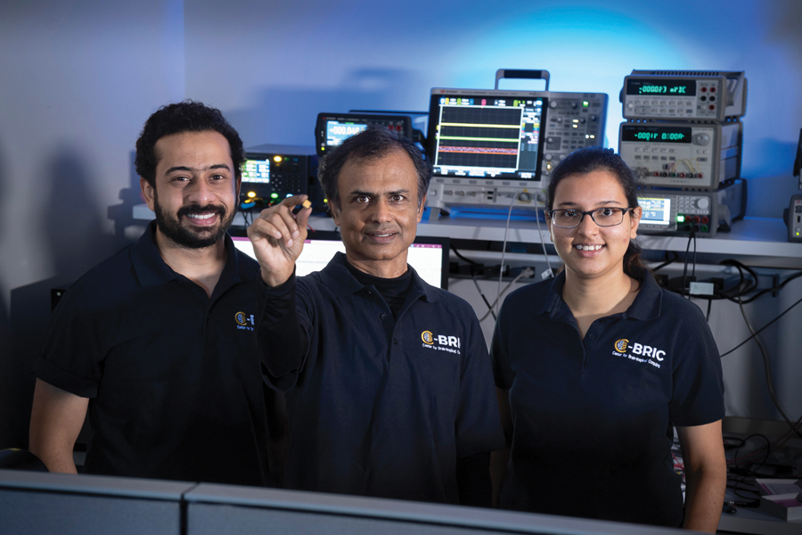
The boundary between memory and processing that was drawn clearly in the early days of computing by von Neumann still defines virtually all modern computing platforms, but the gap between processor and memory speeds has grown to create the daunting "memory wall" that threatens to stymy further progress in computing system performance. Further, the energy cost of moving data between DRAM and processors in the roughly 100 million computer servers in the world exceeds the output of over two Hoover Dams! After decades of progress in computing systems, we must revisit the von Neumann paradigm. Professors Roy and Raghunathan lead research on new approaches to information processing in C-BRIC, the $36M SRC/DARPA Center for Brain-inspired Computing and in the Institute for Cognitive Computing. The goal is to deliver key advances in cognitive computing to enable a new generation of autonomous intelligent systems.
Cognitive computing brings together leading researchers from the fields of machine learning, computational neuroscience, theoretical computer science, neuromorphic hardware, distributed computing, robotics, and autonomous systems. Artificial Intelligence (AI) Hardware, another area of particular strength at Purdue, is also within the scope of the SRC/DARPA Center for Brain-inspired Computing. Eight faculty members from the School of ECE, with an ongoing search targeting two new hires, contribute to this effort. A major part of C-BRIC is focused on compute-in- memory (CiM) for efficient AI and data analytics. Computing-in-Memory (CiM) fundamentally blurs the distinction between processing and memory by bringing them closer, and in the extreme embedding processing capabilities within memory arrays. Besides radically improving the performance and energy efficiency of computing systems, CiM has the potential to enable entirely new categories of products and markets. Purdue researchers have pioneered several advances in the design of CiM systems and demonstrated them through tape outs of chips. A few of the recent tape outs include a 35.5- 127.2 TOPS/W dynamic sparsity-aware reconfigurable-precision Compute-in-Memory SRAM macro for machine learning and a 65nm digital Compute-in-Memory Macro with fused weights and membrane potential for spike-based sequential learning tasks.
Novel Approaches to Information Processing: Probabilistic Spin Logic

Probabilistic Spin Logic (PSL) is a novel approach for information processing that is being explored by a team led by Profs. Datta, Chen, and Appenzeller. The majority of today's digital circuitry is based on building blocks called bits that are deterministically 0 or 1. At the other end of the spectrum are quantum computers consisting of qubits which occupy some superposition of 0 and 1. The probabilistic-bit occupies a niche between these extremes, sharing qualities with both the classical-bit and the quantum-bit. The p-bit fluctuates probabilistically between 0 and 1, and can be pinned to one or the other state based on the magnitude and sign of its input. For a popular description see IEEE Spectrum.
Just as a bit is only useful when in conjunction with other bits, p-bits can be correlated to form p-circuits. These circuits can be programmed to tackle a variety of problems that had been historically reserved to quantum computing, such as optimization, inferencing, and data encryption and decryption—without however the need for ultra-low temperatures. It is in the variety of applications, and the classical nature of the p-bit that this building block comes to life, providing orders of magnitude improvement in performance (see Appl. Phys. Lett.) over standard CPU and GPU implementations.
To date the Purdue team has published many other breakthroughs (for an overview see link), most notably an experimental demonstration of optimization and invertible logic using unstable magnetic tunneling junctions (MTJs), see Nature, and the feasibility of MTJs to demonstrate that complex circuit operations are achievable in realistic hardware systems. This is particularly exciting because it demonstrates the feasibility of fabricating compact energy-efficient hardware p-bits by modifying existing magnetic random access memory (MRAM) technology.
For more information, see: https://www.purdue.edu/p-bit/. To learn about a company commercializing this technology, see: https://ludwigcomputing.com/.
Emerging Logic, Memory, and Interconnect Technologies

Purdue faculty (Alam, Appenzeller, Chen, Janes, and Ye) are actively engaged in the exploration of emerging logic, memory, and interconnect technologies. Purdue's leadership is apparent from the support that these faculty receive from the Semiconductor Research Corporation(SRC) through center-level activities such as the nCORE NEW LIMITS Center (directed by Dr.Chen) and JUMP, where Purdue PIs are involved in the ASCENT Center. In particular, these faculty have focused on experimental demonstrations of the above technologies based on novel materials including low-dimensional materials and ferroelectrics.
Professor Ye has been at the forefront of exploring novel materials for ferroelectric memory applications, and oxide-based channel materials such as In2O3 for back-end-of-line (BEOL) in-memory computing that requires transistors with ultra-low standby power specs and high on-current capabilities. Dr. Ye has worked in strong collaboration with Dr. Alam, who focuses on the reliability physics of these unexplored novel active device elements.
Professors Chen and Appenzeller have experimentally demonstrated that novel low-dimensional materials such as transition metal dichalcogenides (TMDs) with body thickness less than one nanometer can be utilized as channel materials in ultra-high performance transistors and offer performance beyond what silicon technologies can offer. Their work highlights the excellent scalability of devices from TMDs for the next generations of logic computing units. The same sub-1nm thickness also proved highly promising for the use of TMDs as diffusion barriers in future back-end-of-line (BEOL) interconnect technologies. Dr. Chen and Dr. Appenzeller also observed that MoTe2 (a member of the TMD family) based memories give rise to a novel type of phase change switching that is controlled by electric fields. This is a low-power, fast switching memory that combines the characteristics of resistive random access memories (RRAM) and phase change memories (PCM).
These efforts on emerging technologies are enabled by the Birck Nanotechnology Center, which is a state-of-the-art facility that allows prototype fabrication and characterization at scale.
Reliability of Semiconductor Logic and Memory Devices
Under the leadership of Professor Alam, Purdue is well-known for fundamental work on the reliability physics of semiconductor logic and memory devices, both for application-specific consumer electronics and radiation-hardened secure electronics for defense applications. A variety of test equipment available at the Birck Center would support the development of new performance/reliability characterization techniques for DRAM and Flash memories.
It is well known that bit errors (and "repeated-read" security failures) increase significantly as DRAM transistors are scaled below 28-32 nm node because the stored charge at the capacitor node and the leakage through the access transistor are sensitive to transistor scaling. Radiation- induced charge loss and SILC-related gate leakage are concerns that must be addressed. Similarly, next-generation 3D NAND Flash memories will continue to grapple with read-margin, retention, and endurance issues arising from: (a) the threshold-voltage variation due to ambient temperature-sensitivity of polysilicon channel mobility, (b) threshold-voltage fluctuation due to trapping/de-trapping in the tunnel oxides, and (c) the reduced channel cross-section and enhanced field making the bottom cells susceptible to correlated HCI, TDDB, and radiation damages. There is an opportunity to develop more efficient ECC because the bit-flips in 3D NAND Flash are likely to be correlated. Further, for the Compute-in-Memory (CiM) applications involving both logic and memory transistors, classical ECC may not be relevant.
In short, Purdue can support the development of new characterization techniques and physics- based reliability models for HCI, SILC, TDDB, and radiation-related reliability issues of DRAM and Flash memories. These reliability models will be informed by a deep understanding of the cross- layer design considerations, including those arising from heterogenous integration (HI) that defines the thermal and stress-related crosstalk among various components.
Sustainability of Electronic Ecosystems
Sustainability is a core value at Purdue, as evidenced not only in green buildings and clean energy, but also in creating technologies that make the world a better place. Purdue is committed to the "Double Bottom Line" to care for people and the planet through the development of new technologies.
Purdue has a strong tradition in quantifying the economic, environmental, and societal impacts of the decisions made in early-stage R&D; on the ultimate impacts in the realized products and their global supply chains. We welcome collaborations in coupling sustainability R&D; at Purdue with the supply chains, technology developers, and decision-makers of companies. Three examples of recent collaborations that could serve as models are: (1) the DOE Critical Materials Hub in which Purdue provides quantification of both commercialization potential and environmental impact of technologies being developed by researchers from four DOE Labs, ten companies, and eight universities, (3) the iNEMI Project on Value Recovery from End-of-Life Electronics, co-led by Purdue, in which Seagate, Google, Microsoft, Cisco, and others demonstrated nine circular economy technologies for remanufacturing, reuse, and recovery of rare earth magnets in hard drives, and (3) an NSF graduate education and training program on Design for Globally Sustainable Electronics in which DBL is a central tenet, with a customizable curriculum based on partner company needs. For the latter, these courses are part of the new MS in Semiconductors and Microelectronics at Purdue and the undergraduate certificate in Semiconductors.
Finally, Purdue not only has deep expertise in R&D;, but also in workforce development to address issues of local, regional, and global concern, including but not limited to clean energy, smart grids, system design and operation for Net Zero, and developing leadership for creating and operating sustainable systems.
Atomic-Scale Engineering of Semiconductor Materials and Devices

Under the leadership of Professor Ye, Purdue faculty are actively engaged in the exploration of novel electronic materials and devices for post-Moore era semiconductor technologies. One of the utilized technologies is called atomic layer deposition (ALD). ALD is a thin-film deposition technique with atomic-scale controllable accuracy based on the sequential use of a self-limiting chemical process; it is a subclass of chemical vapor deposition. ALD became an enabling technology for the continuation of Moore's law by integrating high-k dielectrics in Si CMOS processes. ALD is a key process in fabricating semiconductor devices in particular as the dimension of state-of-the-art device technology is approaching single-digit nanometer length scales.
In the past decades, we have been working actively on ALD dielectrics and their integration on traditional and novel semiconducting channel materials including Si, Ge, III-V compound semiconductors, 2D materials, and oxide semiconductors. Beyond high-k and higher-k dielectrics, we also have explored ALD-grown ferroelectrics such as HfZrO2 for emerging logic and memory applications. IEDM 2021 (PDF). More recently, we pioneered the use of the ALD technique to form atomically thin oxide semiconductor channels with remarkable performance including unprecedented ultra-high drain currents and transconductances among all field-effect transistors based on any semiconductor materials Nature Electronics 2022 (PDF). ALD interlayers can also be used a phonon spectrum match buffer to enhance the thermal dissipation and electrical-thermal co-design of atomic-scale electronic devices.
Beyond graphene and transition metal dichalcogenides (TMDs) 2D materials research, Purdue faculty pioneered phosphorene ACS Nano 2014 (PDF) and tellurene Nature Electronics 2018 (PDF), two special elemental van der Waals 2D monolayers of phosphorus and tellurium with thickness less than one nanometer. We systematically studied their electrical, optical, thermal, and mechanical properties and their applications for electronic devices. More interestingly, we are able to form a single atomic chain of tellurium atoms towards the smallest semiconductor channel. Nature Electronics 2020 (PDF).
These efforts are enabled by the Birck Nanotechnology Center, which is a state-of-the-art facility that allows atomic-scale nanomaterial synthesis and prototype atomic-scale fabrication and characterization.