Thermoelectric phenomena in semiconductor nanostructures
Thermoelectricity is the inter-conversion of electricity and heat, a phenomena which was discovered in the late 19th century by physicists like Seebeck, Peltier, Thompson, etc. The first formal theory for thermoelectric properties in semiconductors was proposed by Altenkirck and later refined by A. Ioffe.
The thermoelectric efficiency of a material is measured using a quantity called ``Thermoelectric Figure of Merit” given as ZT (proposed by Ioffe and Altenkirck). This details of ZT and the material properties making it are shown in the figure below.
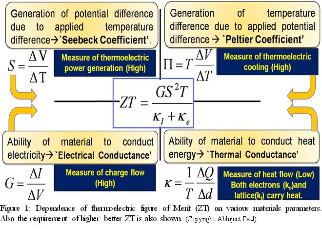
Thermoelectric figure of merit consists of 4 material component as shown in Figure 1. These are
- Electronic Conductance (G): This measures the efficiency of the material to transport electric current. A higher value of G is feasible for higher ZT.
- Seebeck Coefficient(S): This is the measure of how good a material converts heat into electricity.
- Peltier Coefficient(P): This is opposite of S. This quantity measures how good a material converts electricity into heat.
- Thermal conductance(k): This is the measure of heat conduction in a material. In semiconductors this is composed of two part, electronic (ke) and lattice (kl). In semiconductors majority of the heat is carried by the lattice since electron density is less. In metals most of the heat is carried by the electrons.
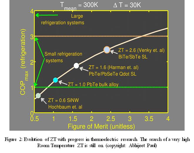
For better thermoelectric performance a higher value of ZT is needed and the search for higher ZT material has been going on for the last 60 years (Fig. 2).
Some of the ways suggested to improve ZT in semiconductors are:
- Using materials with smaller thermal conductivity (kl)
- Using nanostructures to engineer DOS to engineer G and S (proposed by Dresselhaus et. al and Mahan et. al).
- Using Phonon Glass and Electron Crystal (PGEC) which consists of nano-composities, semiconductor superlattices, etc.
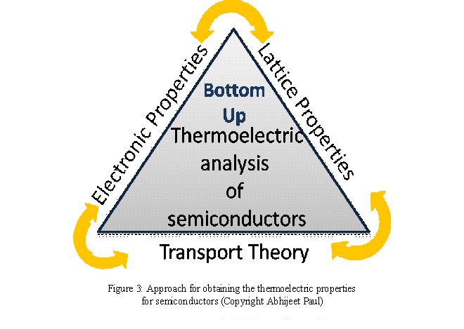
In our group we focus mainly on the methods of nanostructuring, alloying and new materials. In this respect we are exploring in the following directions:
- Impact of nanostructuring on the thermoelectric power factor in Si and GaAs nanowires.
- Effect of strain on thermoelectric power-factor of semiconductor nanowires. See this link
- Exploration of nanostructures made of PbSe, PbTe for thermoelectric efficiency.
- Study the effects of nanostructuring on thermal transport in semiconductors using phonons. For more details see this page
Major Projects in this area:
Associated publications:
- Atomistic modeling of the thermoelectric power factor in ultra-scaled Silicon nanowires, Abhijeet Paul and Gerhard Klimeck, Silicon Nanoelectronics Workshop (SNW),13-14 June 2010 DOI: 10.1109/SNW.2010.5562583
- Enhancement of thermoelectric efficiency by uniaxial tensile stress in n-type GaAs nanowires, Abhijeet Paul, Kai Miao, Ganesh Hegde, Saumitra Mehrotra, Mathieu Luisier and Gerhard Klimeck, submitted to IEEE NANO, 2011.
- Atomistic study of electronic structure of PbSe nanowires, Abhijeet Paul and Gerhard Klimeck, submitted to APL.
Group member involved:
- Abhijeet Paul: Exploration of new materials and nanostructuring on thermoelectric power factor (PF=S2G). Role of strain and superlattices on electrons and phonons.
- Kai Miao: Study the impact strain on the electronic properties of GaAs.