Nanoelectronic Modeling
What is Nanoelectronics?
Nanoelectronic devices are based on structures whose material properties vary on an atomic length scale. Such structures can be created with a variety of experimental methods in a variety of different material systems. Interfaces between different materials can be atomically abrupt. These abrupt interfaces enable device designers to confine electrons quantum mechanically. Interactions/transitions between different man-made quantum mechanical states open a cornacopia of new device applications.
What are the Applications?
- Lasers: Electrons in higher energetic states can emit photons by a transition to lower energetic states.
- Detectors: Electrons can be excited by a photon to junp from a lower to a higher energetic state.
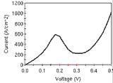
- Logic/Memory: Electrons can transition without loss of energy from one quantumj state to the next by quantum mechanical tunneling. The speed of such electronic transport can be very high leading to new low power and high density devices.
Why Modeling?
Device simulation based on semi-classical approximations has proven to be a crucial element in the success of the semiconductor industry. The now available nanoelectronic design space has increased due to the large number of material systems and design concepts. However the standard simulation tools for electronic devices brake down since they do not incorporate quantum mechanical effects.
What is NEMO?
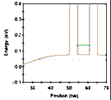
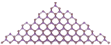
NEMO-1D and NEMO-3D are quantum mechanical based simulation tools created to provide quantitative predictions for nanometer scaled semiconductor devices. NEMO-1D is based on the non-equilibrium Greens function formalism incorporating full bandstructure, scattering and charging effects. NEMO-1D has been used extensively to investigate and design resonant and esaki tunnel diodes, quantum well optical detectors and emitters, and gate oxide leakage in ultra-scaled CMOS. A 3D extension to NEMO is currently under construction at JPL. This simulator computes strain field, quantum states, and optical matrix elements using an atomistic tight-binding Hamiltonian. Target applications for NEMO-3D include semiconductor quantum dots and molecular-based electronics.
NEMO-1D History:
NEMO-1D was originally developed at Texas Instruments and Raytheon with U.S. government funding. The tool was delivered to the U.S. government and it is available to the U.S. research community.