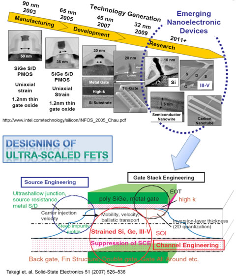
Ultra-Scaled FETs
CMOS scaling has been the mainstay of the semiconductor industry for last few decades. MOSFET channel lengths have been scaled from about few microns length in the 1990's to about ~ 25 nm by 2009. However as we shrink channel lengths further below 20 nm new device designs and materials are needed to sustain the device performance.
In this group we work on different aspects of transistor designs that range from new transistor designs i.e. Tunnel FETs to usage of new materials i.e III-V,SiGe etc.
Capabilities we have:
- 3D full-band quantum transport simulator based on the atomistic tight-binding theory.
- 2D semi-classical top-of-the-barrier using atomistic tight-binding theory.
Topics we work on:
- III-V based NMOS transistor designs – HEMT’s, Multigate-FET’s.
- SiGe/Si based PMOS devices – UTB/Nanowire MOSFETs
- Si nanowire FETs
- Tunnel FETs – using band to band tunneling to achieve <60 mV/dec
- Collaborate with experimentalists in providing a theoretical understanding.
- etc.
Group Members involved
- Mathieu Luisier
- Abhijeet Paul
- Saumitra Mehrotra
- SeunGeun Kim
- SeungHyun Park
- Mehdi Salmani
- Woo-Suhl
- Kai Miao
- Samarth Agarwal
- Neerav Kharche