Electron-Phonon Scattering in NW FETs
| Electron-Phonon Scattering in NW FETs |
Mathieu Luisier, Gerhard Klimeck |
|
Objective:
- Solve one of the Grand Challenge problems in device simulation: the simultaneous inclusion of an atomistic description of the simulation domain, a full-band description of the materials, and electron-phonon scattering
Approach:
- Use of the sp3d5s* tight-binding model to describe electrons and holes
- Use of the Non-equilibrium Green's Function (NEGF) formalism to solve quantum transport
- Electron-phonon scattering in the self-consistent Born approximation
- Efficient multi-level parallelization scheme
Results and Impacts:
- Modification of current distribution and band edges and reduction of drain current
- First dissipative quantum transport simulations of realistically extended nanowire transistor structures
Ongoing Work:
- Mobility extraction in n- and p-doped nanowires with different crystal orientations
- Look for experimental data to verify the model
|
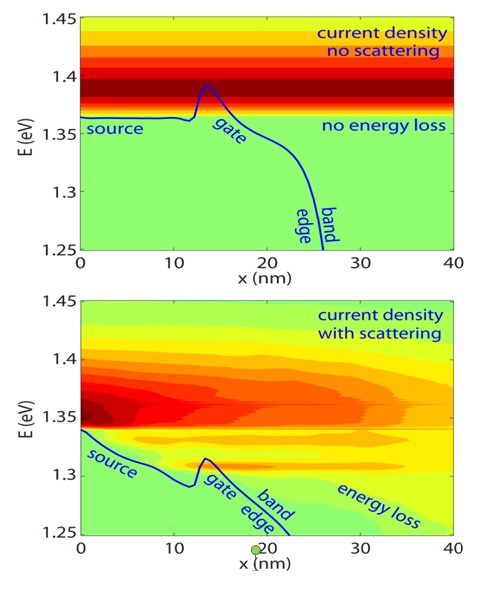
Image Caption:
- Energy-resolved current distribution in a nanoscale NW FET.
Up: coherent transport without energy loss. Down: with phonon scattering. Energy loss and source access resistance.
|
Powerpoint slide as ppt, pdf, or as image below.
