Phase Transition Material based Low Power Device-Circuit Design
Hyper-FET / Phase-FET:
Hybrid phase transition FET (Hyper-FET) is a very recent inclusion in the family of steep (< 60 mV/dec) switching transistors. This novel transistor comprises of a correlated material [1] or in general term, threshold switch [2] augmented to the source terminal of a regular transistor (MOSFET or FinFET). The current driven abrupt phase transition of the threshold switch leads to abrupt (not instantaneous) switching in the transistor itself and can overcome the Boltzmann limit [1].
The idea was first reported and demonstrated in [1] with a hybrid arrangement (wire connected) between Vanadium dioxide (VO2) (a well-known threshold switch) and a bulk transistor. Next year, monolithic integration of VO2 on source contact of a transistor was reported [3] and the name Phase-FET was used instead of Hyper-FET (as hybrid arrangement was no longer required). Our group contributed to the development of the idea through modeling and simulation support. We also established and reported device-circuit co-design methodology for this novel transistor technology [4, 5]. We also contributed to the development of Ag-HfO2 based Phase-FET [2] through modeling and simulation-based insights. A novel SRAM structure based on Phase-FETs was also proposed and analyzed by our group [6].
References:
[1] N. Shukla, et. al., “A steep-slope transistor based on abrupt electronic phase transition,” Nature Communications, Aug. 2015.
[2] N. Shukla, et. al., "Ag/HfO2based threshold switch with extreme non-linearity for unipolar cross-point memory and steep-slope phase-FETs," 2016 IEEE International Electron Devices Meeting (IEDM), 2016.
[3] J. Frougier, et. al., "Phase-Transition-FET exhibiting steep switching slope of 8mV/decade and 36% enhanced ON current," 2016 IEEE Symposium on VLSI Technology, 2016.
[4] A. Aziz, et. al., "Steep Switching Hybrid Phase Transition FETs (Hyper-FET) for Low Power Applications: A Device-Circuit Co-design Perspective–Part I," in IEEE Transactions on Electron Devices, 2017.
[5] A. Aziz, et. al., "Steep Switching Hybrid Phase Transition FETs (Hyper-FET) for Low Power Applications: A Device-Circuit Co-design Perspective—Part II," in IEEE Transactions on Electron Devices, 2017.
[6] S. Srinivasa, et. al., "Correlated Material Enhanced SRAMs With Robust Low Power Operation," in IEEE Transactions on Electron Devices, 2016.
Cross-point Memory Array and Selector Design:
Cross-point architecture is a concurrent technique to achieve high density non-volatile memory storage [1]. This architecture utilizes orthogonally running metal lines (named as bit lines and word lines). The memory elements (Magnetic tunnel junction, Phase change memory or Resistive RAM) are sandwiched between the metal lines. The use of access transistor is averted and the memory elements can be fitted within the metal footprint. Thus a very high integration density is achieved. However, to select/deselect specific memory cells and to suppress sneak current paths across the array, it is important to use switches with high ON/OFF ratio (> 107) in series with each memory element [2]. These switches are called selectors. Threshold switches [3] are a popular type of selector which are being explored and studied with importance to improve and optimize the cross-point array design.
We have established a framework for simulating and exploring the design space of cross-point array with threshold switch type selectors [3, 4]. We use that framework to explore the implications of sever threshold switching materials. We also have established figures of merit to determine the usability of a threshold switching material as a selector, considering several interdependent design constraints. In addition, we developed a computationally efficient compact model [5] to estimate the leakage current/power in a cross-point array. The leakage in a cross-point array is one of the main factors that limit the array size as well as the robustness of the read operation, keeping aside the obvious implication in power penalty. But estimation of these leakage components traditionally required simulation of the entire array and used to claim a lot of computational resources. Our compact model provides a unique opportunity for quick estimation of leakage and therefore is very useful for optimization and iterative design. We also provided modeling and simulation support for the development of a novel three-terminal selector based on Vanadium dioxide (VO2) which has the potential to enable new biasing schemes and relax the design constraints [6].
References:
[1] S. K. Gupta, et. al., "On the potential of correlated materials in the design of spin-based cross-point memories (Invited)," 2016 IEEE International Symposium on Circuits and Systems (ISCAS), 2016.
[2] N. Shukla, et. al., "Ag/HfO2based threshold switch with extreme non-linearity for unipolar cross-point memory and steep-slope phase-FETs," 2016 IEEE International Electron Devices Meeting (IEDM), 2016.
[3] A. Aziz, et. al., "Analysis of Functional Oxide based Selectors for Cross-Point Memories," in IEEE Transactions on Circuits and Systems I: Regular Papers, 2016.
[4] A. Aziz, et. al., "Implication of hysteretic selector device on the biasing scheme of a cross-point memory array," 2015 International Conference on Simulation of Semiconductor Processes and Devices (SISPAD), 2015.
[5] A. Aziz, et. al., "A computationally efficient compact model for leakage in cross-point array," 2017 International Conference on Simulation of Semiconductor Processes and Devices (SISPAD), 2017.
[6] A. Aziz, et. al., "A Three-Terminal Edge-Triggered Mott Switch," 2018 76th Device Research Conference (DRC), 2018.
Threshold Switch Augmented Spin Memories:
Spin transfer torque (STT) MRAM is one of the most prominent non-volatile memories in current electronic industry. They provide high integration density, zero standby leakage, impressive thermal stability, high retention and endurance. However, a well-known limitation for these devices is the relatively low sense margin and the read/write conflicts. It is difficult to improve the distinguishability of stored data (low and high digital states) without hurting the stability and robustness of read operation. In addition, asymmetry in low-to-high and high-to-low write operation poses concerns regarding power penalty.
We proposed a technique of augmenting threshold switching materials with the STT MRAM which could improve the distinguishability and robustness of read operation simultaneously [1]. This unique MRAM structure was first names as- Correlated material assisted STT MRAM (COAST) [1]. As the design can be realized using any threshold switching material (correlated oxides, filamentary conductors, doped chalcogenides etc.), the name was later generalized as Threshold switch augmented STT MRAM (TSA-MRAM) [2]. We proposed a different technique [3] for MRAMs with separate read/write paths (SRWP) which would be suitable for high-speed current based sensing. This version had phase transition material augmented in parallel with the magnetic tunnel junction and hence was short-named: PA-PTM SRWP MRAM. Even though both designs utilize the selective phase transitions in threshold switching materials, the principle of operation and design mechanism are significantly different for these techniques [4].
References:
[1] A. Aziz, et. al., "COAST: Correlated material assisted STT MRAMs for optimized read operation," 2015 IEEE/ACM International Symposium on Low Power Electronics and Design (ISLPED), 2015.
[2] A. Aziz et. al., “Threshold Switch Augmented STT MRAM: Design Space Analysis and Device-Circuit Co-design," to appear in IEEE Transactions on Electron Devices, 2018.
[3] A. Aziz, et. al., "Read optimized MRAM with separate read-write paths based on concerted operation of magnetic tunnel junction with correlated material," 2015 73rd Annual Device Research Conference (DRC), 2015.
[4] A. Aziz et. al., "Read-enhanced spin memories augmented by phase transition materials (Invited)," 2017 IEEE 60th International Midwest Symposium on Circuits and Systems (MWSCAS), 2017.
Threshold Switch Augmented Peripheral and Analog Circuits:
The abrupt current driven phase transitions and orders of magnitude difference between metallic and insulating states of a threshold switch, enable unique opportunities to use them in designing novel circuits. We proposed a current based sense amplifier [1] capable of generating and tuning its own reference utilizing the properties of threshold switch/phase transition material. This design requires significantly less area than conventional current based sense amplifier. We proposed a Cockcroft-Walton Multiplier (creates large DC voltage from pulsating AC voltage) based on unipolar threshold switches [2] which could achieve up to ~50% higher DC output compared to conventional design. We envisioned that the unipolar threshold switch might act as a hysteretic diode and utilized this unique feature to alleviate the diode drop.
References:
[1] A. Aziz, et. al., "Low power current sense amplifier based on phase transition material," 2017 75th Annual Device Research Conference (DRC), 2017.
[2] A. Aziz, et. al., "Cockcroft-Walton Multiplier based on Unipolar Ag/HfO2/Pt Threshold Switch," 2018 76th Device Research Conference (DRC), 2018.
Phase Transition Materials Enhanced SRAMs and DRAMs:
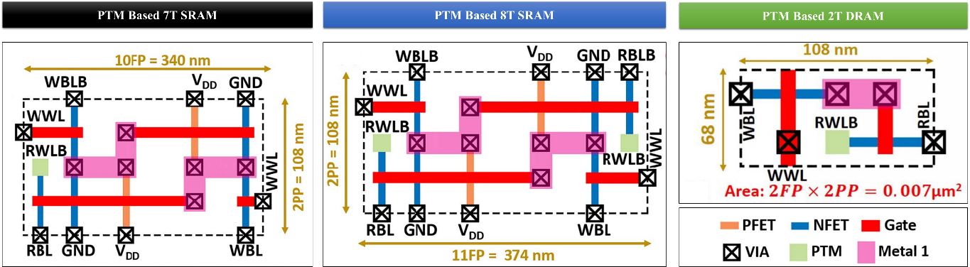
The unique properties of phase transition materials (PTM) can be harnessed to design enhanced SRAMs and DRAMs. We proposed three versions of memories with separate read-write paths augmented by PTM [1, 2]. the variants are: a) 7T SRAM with single ended read; (b) 8T SRAM with differential read and (c) 2T DRAM. These memory bit-cells augmented by PTMs enable separation of read and write paths with lower area compared to standard multiport memories (such as 8T SRAMs and 3T DRAMs). The benefits of the separation of read–write paths in memories in terms of mitigating design conflicts have been proven in multiple works in the past. However, additional transistors required for read–write path separation incur area penalty. By utilizing the abrupt phase transitions and orders of magnitude difference in the insulating and metallic resistances of the PTM, we showed that the read port could be designed without a read access transistor, and without employing any read assist technology. Thus our technique led to more efficient designs. The read performance of our proposed 8T cell showed a 38% improvement compared to previously proposed standard 8T design. Similarly, our 2T DRAM cell achieved 20% less cell area than 3T DRAM, with less than 6% read time penalty. The benefits for all the designs came at no write overheads.
References:
[1] Z. Shen, S. Srinivasa, A. Aziz, S. Datta, V. Narayanan and S. K. Gupta, "SRAMs and DRAMs with Separate Read–Write Ports Augmented by Phase Transition Materials," in IEEE Transactions on Electron Devices, vol. 66, no. 2, pp. 929-937, Feb. 2019.
[2] S. Srinivasa, A. Aziz, N. Shukla, X. Li, J. Sampson, S. Datta, J. Kulkarni, V. Narayanan and S. K. Gupta, "Correlated Material Enhanced SRAMs With Robust Low Power Operation," in IEEE Transactions on Electron Devices, vol. 63, no. 12, pp. 4744-4752, Dec. 2016.