TMD Interconnects
Modeling and Benchmarking of 2D TMD interconnects:
|
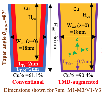
Interconnect scaling is one of the key challenges for several reasons. First it reduces the copper cross-sectional area for conduction and increase copper resistivity due to sidewall scattering and grain-boundary scattering. Second, the highly resistive barrier/liner (TaN/Ta) layers further reduce the cross-sectional area of Cu. Third, the forward mentioned barrier/liner are in the path of the vertical conduction through the vias, which significantly increases the via resistance. To address some of these challenges, replacing the conventional TaN/Ta with ultra-thin 2D transition metal dichalcogenide (2D TMD) material TaS2 has been proposed. With only 0.7nm of TaS2 (as opposed to 2nm TaN + 2nm Ta), we can observe significant increase in Cu volume. However, TaS2 suffers from higher vertical resistivity compared to TaN/Ta, which deteriorates the via conductivity. Therefore, evaluation of the overall performance of TMD-augmented interconnects mandates extensive device modeling and circuit analysis. |
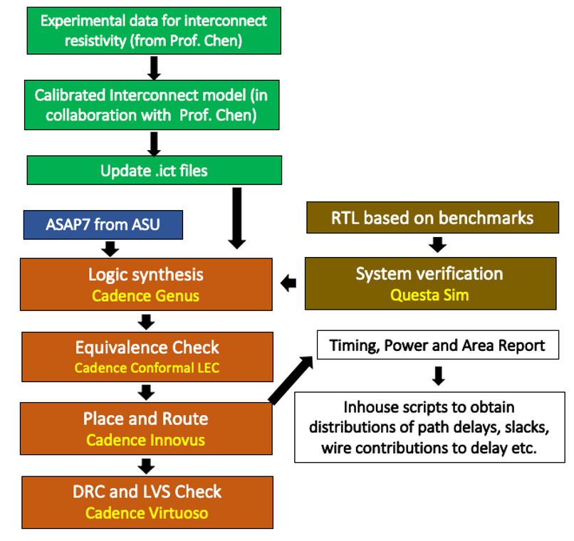
Benchmarking Flow
...
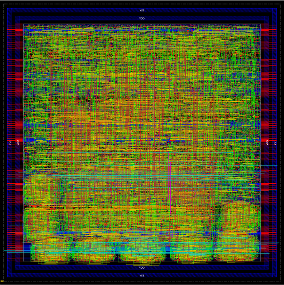
Final GDSII Layout of AES circuit
...
Effective frequency vs TaS2 vertical resistivity
...