Research
The four key thrusts of research are: (a) renewable energy materials (b) heterogeneous integration and advanced semiconductor packaging (c) in-situ and in-operando testing and characterization (d) materials sustainability. A few example projects are included in each research thrust.
 Renewable Energy
- Metastability and long-term degradation of halide perovskite and chalcogenide thin-film PV.
- Wide bandgap p-type materials for tandem and bifacial solar cells
- Development of stable and sustainable Pb-free halide perovskites and chalcogenide for PV and PEC applications.
-
1D/2D/3D halide Pb-free perovskite heterostructures PEC devices for H2 production
 Semiconductor Packaging
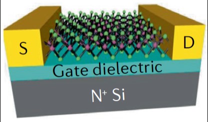
- High lifetime electrical contacts for 2D semiconductors for BEOL integration.
- Electro-thermo-mechanical reliability of embedded contacts and interconnects.
- Novel materials and package architectures for electro-thermo-mechanical reliability of high temperature sensors and electronics.
- Reliable and fine pitch on-chip and off-chip interconnects.
- Reliability of thermal interface materials in immersion cooling systems.
- Reliability of Pb-free high temperature solders.
 In-situ Accelerated Stress Testing
- Application of in-situ and in-operando characterization methods to identify degradation modes and understand the underlying degradation mechanisms.
- Metastability and degradation in thin-film PV.
 Materials Sustainability
- Recovery of critical metals/non-metals/semiconductors through sustainable extraction methods.
 Workforce Development:
- Identify technology growth vectors in Advanced Semiconductor Packaging, and develop opportunities for student training programs.