Research
Wireless Micro-Electrode Arrays
Research in neuroscience and cell biology have long benefitted from microelectrode arrays (MEAs). Approaches to link electro-physiological measurements with other quantitative cell properties have started to surface. The idea is to develop an extremely flexible active MEA chip with hundreds of electrodes that is wirelessly powered and communicated with. On the neural prosthesis front, the proposed wireless active MEA will be a leap in technology as it can achieve excellent sensitivity for hundreds of recording electrodes integrated on a single chip. Examples of the active MEA technology at Purdue are shown below.

Brain Implant Technology
The wireless MEA technology can be used to monitor brain activity.

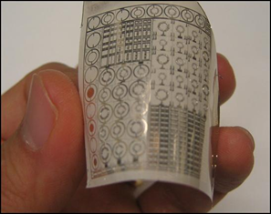
Flexible Electronics
SiVIC group is a pioneer in flexible electronics based on Carbon Nanotube transistors and organic LEDs for flexible transparent displays. We have also demonstrated flexible integration using our previously patented SAWLIT technology. More recently, we have focused on developing solution-based oxide semiconductors such as IZTO and IGZO for thin film transistor applications. This area is expanding and we hope to be able to demonstrate MHz to GHz TFTs using printable electronic technology.
Fluidic Nano-Channels
Fluidic micro and nano-channels are created using post CMOS processing and have a variety of applications including detection, and characterization of cells, bacteria and viruses in a fluidic media. The following figure shows different types of fluidic nanochannels that have been developed in our group. Both CMOS horizontal fluidic nanochannel with transverse electrodes (U.S. patent 8,907,684) and the so-called perforated MOS vertical fluidic nanochannel device (U.S. patent 9,188,563) have been designed and fabricated. We currently have two active projects that are utilizing these devices. In one project, we look to detect cancer cells and distinguish them from normal cells in a fluidic media. In the second project, different viruses are measured for their bio-impedance and they are detected and classified based on the features extracted from their bio-impedance. This technology allows instant testing for viral infection such as Covid 19 in a matter of few minutes.
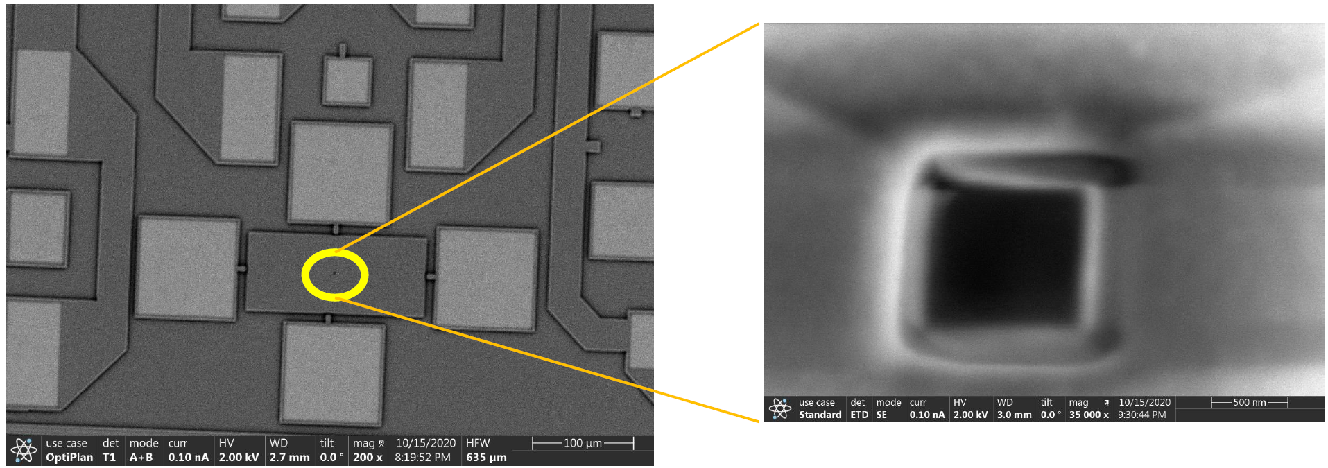
Integrated Nano Electromechanical Structures (NEMS)
Suspended Si and metal nanowires implemented in CMOS technology can be used as high quality factor (Q~3000 in vacuum) nano-electromechanical resonators with slight frequency tuning capabilities. These post-processed CMOS-based devices are repeatable, reproducible and have high yields, which make them suitable for a variety of circuit applications. Chief among them are integrated filters, mixers and local oscillators. The Figure shows examples of NEMS and MEMS devices that are post-processed using a GlobalFoundries 45 nm CMOS SOI technology. This work has received global news coverage through NSF and other scientific news outlets.
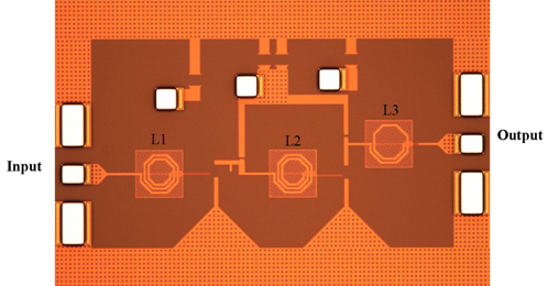
RF to MM-Wave Transceivers
HINET has used a novel design technique (U.S. patents 9,190,269, 8,558,619, 8,368,469) to implement CMOS SOI power amplifiers for 4G, 5G and WiGig standards. Using this technique, the group has achieved the highest output power from a CMOS chip at RF frequencies (low GHz range) and also at microwave frequencies, and the highest power-added efficiency (PAE = 42% at 46 GHz) reported to date for CMOS-based mm-wave PAs. The research is moving towards high performance single-chip front-end transceiver design for RF to mm-wave applications (4G, 5G and WiGig standards).