Projects
Density Function Renormalization Group and Quantum Monte Carlo studies of extended Kitaev model at high temperatures
Team: Vahagn Mkhitaryan, Owen Maxwell Matthiessen
Brief Description
Kitaev model is an exactly solvable model of interacting spin on a honeycomb lattice with bond dependent anisotropic interactions proposed by Alexei Kitaev in 2006 [1]. The model is described by the Hamiltonian:
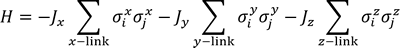
A few years after Kitaev introduced the honeycomb model, G. Jackeli and G. Khaliullin proposed a path to realization of such models in real materials using strong spin orbit coupling in partially filled d-shell transition metal compounds with octahedron arrangement of constituent atoms [2]. Several candidate materials have been found since then that could realize this model [3]. Although Kitaev interaction terms in most of the candidate materials are dominant, it is still an effective spin model and other types of interactions play a significant role in these materials and they need to be considered in real experimental data interpretation [4]. In this study we will use Density Matrix Renormalization Group (DMRG) and Quantum Monte-Carlo (QMC) approach to study extended Kitaev model and its temperature dependent properties. The focus is on derivation of inelastic light scattering intensities for the extended Kitaev model and analyzing it at various temperatures and applied external magnetic field strengths.
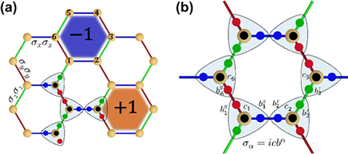
Figure The Kitaev honeycomb model. a) schematic representation of the honeycomb lattice of spins S=1/2 with bond-dependent interactions. b) Majorana fermion representation of the spin operators and interactions in Kitaev model
References
[1] Kitaev A 2006 Anyons in an exactly solved model and beyond Ann. Phys. 321 2–111
[2] Jackeli G and Khaliullin G 2009 Mott Insulators in the Strong Spin-Orbit Coupling Limit: From Heisenberg to a Quantum Compass and Kitaev Models Phys. Rev. Lett. 102 017205
[3] Trebst S and Hickey C 2022 Kitaev materials Phys. Rep. 950 1–37
[4] Motome Y and Nasu J 2020 Hunting Majorana fermions in Kitaev magnets J. Phys. Soc. Jpn. 89 012002
Optical Probing and Tailoring of Optical Properties in Weyl Semimetals
Project Team: Morris Yang (Lead), Demid Sychev
Weyl semimetals (WSMs) are an emerging class of materials possessing unique electromagnetic properties that are not commonly achievable with conventional metals and semiconductors. The exotic phenomena, emerging from the so-called Weyl nodes in WSMs where valence and conduction bands cross in single points and electrons effectively behave as Weyl fermions, make WSMs very interesting for novel photonic applications in the areas of non-linear optics, photovoltaics, THz electrooptics, and detection. In this work, we explore the enhancement of WSM nonlinear response by merging WSMs with the concept of plasmonics, i.e. nano-optics utilizing deeply subwavelength collective oscillations of free electrons in metallic nanostructures, and metasurfaces where arrays of plasmonic nanoantennas are used to control the phase, amplitude and polarization of the incident light. Since electrons possess non-trivial electronic states in WSMs, plasmonics could enable the observation of unique optoelectrical phenomena in WSMs with the added benefit of creating nonlinear optical elements that are smaller than the diffraction limit. Here, we realized a nanopatch plasmonic antenna array on the WSM TaAs crystal to demonstrate the enhanced non-linear optical response from TaAs. By developing a large-scale, non-destructive method of fabricating the antenna array, we address the challenge of WSM integration with photonic devices. We demonstrate a six-fold increase of the second-harmonic generation (SHG) from the Weyl semimetal TaAs surface by distributing plasmonic silver nanoantennas on TaAs.
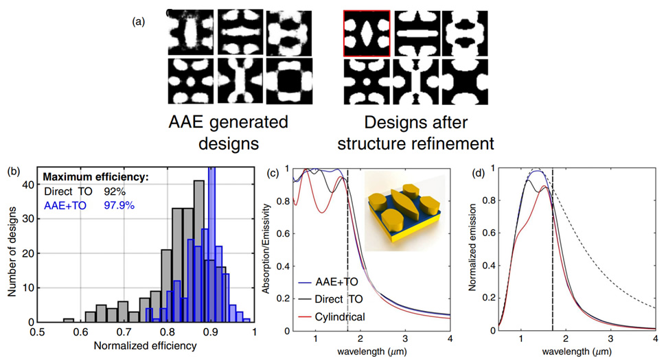
3-D Topological Optimization with Gradiently Changing Index Materials for Electromagnetic Inverse Design
Project Lead: Omer Yesilyurt
Brief Descripton:
Topology optimization methods have gained significant popularity in recent years for the inverse design of nano-photonic systems. These methods are available in various forms and have been presented under different names. The approaches involve using gradient and non-gradient based algorithms, along with systematic techniques to improve convergence, solution discreteness, and manufacturing constraints. More recently, data driven methods such as Machine Learning has also been involved in inverse photonic design.
Traditionally, the inverse designed structures are complex in only 2 directions since optimization in the thickness direction would result in unfabricable optical devices. Here, we propose a novel inverse design technique that incorporates the 3rd dimension into photonic inverse design using adjoint topology optimization and deep neural networks in tandem. The method uses adjoint topology optimization for the transverse direction and deep learning to optimize gradiently changing multilayer film in the thickness direction. We believe this method is going to enable a completely new family of devices and design techniques across all electromagnetic structures.
Project Publications:
[1] Omer Yesilyurt, Zhaxylyk A. Kudyshev, Alexandra Boltasseva, Vladimir M. Shalaev, and Alexander V. Kildishev ACS Photonics 2021 8 (10), 3061-3068 DOI: 10.1021/acsphotonics.1c01070
[2] Yesilyurt, Omer, Peana, Samuel, Mkhitaryan, Vahagn, Pagadala, Karthik, Shalaev, Vladimir M., Kildishev, Alexander V. and Boltasseva, Alexandra. "Fabrication-conscious neural network based inverse design of single-material variable-index multilayer films" Nanophotonics, 2023. https://doi.org/10.1515/nanoph-2022-0537
Deep Learning Based Superconducting Qubit Readout
Project Team: Omer Yesilyurt (in collaboration with Dr. Alex Ma Group and Fermilab)

Brief Descripton:
In the field of quantum computing, reading a qubit is a crucial operation that involves converting quantum information into classical information. This enables subsequent classification, where the qubit states are assigned as either '0' or '1'. Unfortunately, qubit readout is a challenging and time-consuming process, particularly on superconducting quantum processors. The most cutting-edge superconducting quantum processors are prone to readout errors, with a range of 1-10%. These errors are caused by a variety of factors, including crosstalk, spontaneous state transitions, and excitation due to the readout pulse. Given the error-prone nature of the readout process, extensive research has been conducted to develop better discriminators that can achieve higher qubit-readout accuracies. In this project, we develop novel deep learning techniques aimed at improving the fidelity of state readout in superconducting qubit systems. Our primary objective is to enhance the accuracy of the readout process. Additionally, we aim to explore the potential of neural networks in identifying and extracting physical information related to the sources of errors in the system.
Machine learning-assisted rapid classification and prediction of single photon emitters
Project Team: Yuheng Chen, Blake Wilson, Daksh Singh, Zachariah Martin
Brief Descripton:
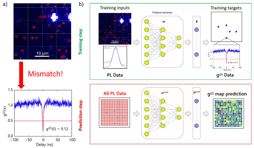
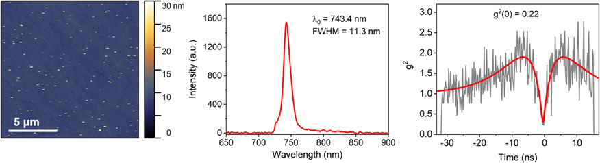
Integrated quantum photonics has recently emerged as one of the key enablers for quantum information science and technology [1]. Successful implementation of quantum photonic devices based on quantum emitters depends crucially on the selection of these emitters from a large inhomogeneous set. It requires efficient identification of bright, stable single-photon emitters with fast emission rates, high quantum yield, and narrow optical linewidth. To characterize single-photon emitters, we have the photoluminescence (PL) mapping method, which is a fast and large-area scanning, but hard to judge the quality of the emitter. Also second-order autocorrelation (g(2)) method is a cornerstone measurement to distinguish “single” or “not-single” of emitters, but particularly time-consuming to realize on a large scale [2-4].
To overcome the efficiency mismatch between the large-scale PL mapping and precise g(2) measurement, we develop a supervised convolutional neural network (CNN) based regression model to realize rapid classification and prediction of quantum emitters. Utilizing both PL spectra and g(2) data of sampled single photon emitters in the training step, we explore the potential correlation between them and predict all-map g(2) measurement in the prediction step to classify whether the emitters are “single” or “not-single”, and further enable super-resolved imaging and scalable assembly of quantum devices.
References:
[1] Simmons, M., 2015. npj Quantum Inf., 1, 15013.
[2] Senichev, A., Martin, Z.O., Peana, S., Sychev, D., Xu, X., Lagutchev, A.S., Boltasseva, A. and Shalaev, V.M., 2021. Room-temperature single-photon emitters in silicon nitride. Science Advances, 7(50), p.eabj0627.
[3] Senichev, A., Peana, S., Martin, Z.O., Yesilyurt, O., Sychev, D., Lagutchev, A.S., Boltasseva, A. and Shalaev, V.M., 2022. Silicon nitride waveguides with intrinsic single-photon emitters for integrated quantum photonics. ACS Photonics, 9(10), pp.3357-3365.
[4] Kudyshev, Z. A., Bogdanov, S. I., Isacsson, T., Kildishev, A. V., A.S., Boltasseva, A. and Shalaev, V.M., 2020. Rapid classification of quantum sources enabled by machine learning. Adv. Quantum Technol., 3, 2000067.
Physics-driven generative adversarial networks (GAN) for the cryptographic chip package
Project Team: Yuheng Chen, Blake Wilson, Daksh Singh, Jaxon Pottle, Sarah Chowdhury
Brief Descripton:
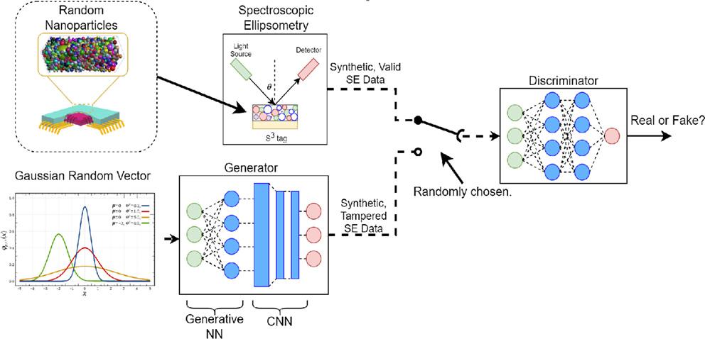
Today’s global microelectronics ecosystem is facing challenging problems of assurance, which focus on decreasing the probability of security vulnerabilities introduced into products without being detected and enabling secure protection against external malicious tampering on chips. One solution is to use steganographic and covert tags with chromatic or polarization encryption (engineered plasmonic color holograms). Despite some substantial theoretical and experimental progress in the physically unclonable functions (PUFs) based on structural color materials, [1-3] it is still a great challenge to achieve a cost-effective structural color assurance tag fabricated through a stochastic process.
To reduce the cost and improve security, we propose the theoretical study and simulation of verifying embedded random plasmonic fillers with a Synthetic Spectral Signature (S3) correlated with stochastic metrics of their structural dimensions and optical properties. To robustly detect the S3 tags made by doping conventional fillers with plasmonic nanoparticles, we propose using variable angle spectroscopic ellipsometry (VASE) that could be challenging without auxiliary data. To decrease such a risk, we propose designing and training a physics-driven generative adversarial networks (GAN) that provides a reliable solution to the inverse problem of covert assurance and a range of discernible plasmonic fillers, enabling secure protection against tampering. Simultaneously, we also utilize computer vision techniques to analyze the distribution mode of the plasmonic fillers revealed by the dark-field microscope. By enhancing S3 discrimination techniques with novel data-driven approaches, we could expand its existing capabilities into the microelectronics assurance domain, thus solving a problem of global importance.
References:
[1] Song, M., Wang, D., Kudyshev, Z. A., Xuan, Y., Wang, Z., A.S., Boltasseva, A., Shalaev, V.M and Kildishev, A. V., 2021. Enabling optical steganography, data Storage, and encryption with plasmonic colors. Laser & Photonics Reviews, 15, 2000343.
[2] Song, M., Wang, D., Peana, S., Choudhury, S., Nyga, P., Kudyshev, Z.A., Yu, H., A.S., Boltasseva, A., Shalaev, V.M and Kildishev, A. V., 2019. Colors with plasmonic nanostructures: A full-spectrum review. Applied Physics Reviews, 6, 041308.
[3] Arppe, R., Sørensen, T.J., 2017. Physical unclonable functions generated through chemical methods for anti-counterfeiting. Nat. Rev. Chem., 1, 0031.
Metalens Array for Rydberg Atom Traps
Project Team: Blake Wilson, Yuheng Chen, Brandon Triplett, Daksh Singh, Vahagn Mhiktaryan, Sam Peana
Brief Descripton:
Achieving fault-tolerant quantum computing requires gate fidelity to reach a threshold of 99.9995% [1]. While modern Rydberg atom systems offer a promising platform, the inefficiencies of spatial light modulators (SLMs) limit their gate fidelity. The reconfigurability of SLMs is crucial for controlling dynamics during computation, however static computer architectures, like those with static memories, make the SLM reconfigurability unnecessary. In this project, we propose using metalenses to trap static Rydberg atoms, which can push gate fidelity closer to the required threshold by maximizing trapping efficiency. The proposed metalens design will be simulated using FDTD and RCWA simulations, optimized to minimize losses due to absorption using machine learning approaches, and is expected to be less complex and more cost-effective than SLMs.
By replacing SLMs with metalenses, we can improve trapping efficiency, which will lead to higher gate fidelity and bring us closer to the threshold for fault-tolerant quantum computing. The metalenses have the potential to offer a simpler, cheaper, and more efficient alternative for trapping Rydberg atoms in static computer architectures.
References:
[1] Yuval R Sanders et al 2016 New J. Phys. 18 012002
[2] Ebadi et al Nature, Volume 595, Issue 7866, p.227-232
Generative Modeling for Quantum Dynamics in Rydberg Atoms
Project Team: Blake Wilson, Vahagn Mhiktaryan
Brief Descripton:
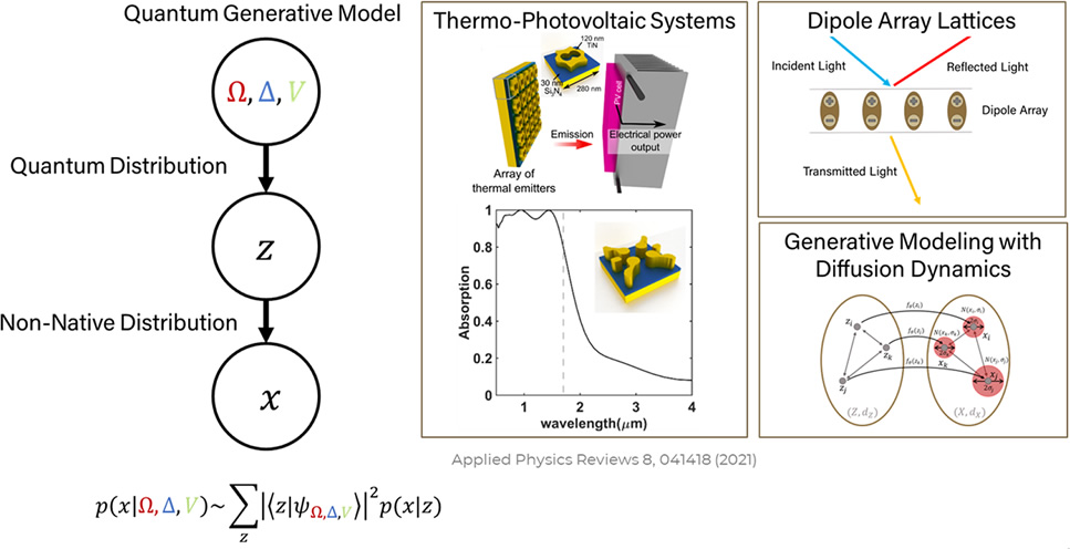
Recent work in Rydberg atom quantum computers and sampling algorithms literature shows promise toward sampling advantages with Rydberg systems [1,2]. To achieve efficient quantum sampling for engineering problems, we propose a machine-learning-based, generative modeling framework utilizing binary variational autoencoders (VAEs) in the context of quantum dynamics in Rydberg atom quantum computing [3]. Specifically, we propose a latent mapping from Rydberg states on lattices to the desired sample space. This allows for complex dynamics in the sample space via the Rydberg states. To further preserve the local structure in the proposed framework, we will use a metric that quantifies the similarity between generated samples and the latent space. By preserving local structure under quantum dynamic processes, this framework seeks to leverage the potential of Rydberg systems in quantum sampling. The proposed framework will be used to generate samples for optimization. The binary VAEs will be optimized using gradient-based optimization methods, and the quantum dynamic processes will be simulated using Bloqade and QuEra’s Rydberg atom quantum simulator.
References:
[1] H. Levine, A. Keesling, G. Semeghini, A. Omran, T. T. Wang, S. Ebadi, H. Bernien, M. Greiner, V. Vuletić, H. Pichler, and M. D. Lukin, " Parallel implementation of high-fidelity multi-qubit gates with neutral atoms," Phys. Rev. Lett. 123, 170503 (2019)
[2] Ebadi et al Nature, Volume 595, Issue 7866, p.227-232
[3] Khoshaman et al arXiv:1802.05779 [quant-ph]
Quantum Bayesian Optimization with Rydberg Atoms
Project Team: Blake Wilson, Vaishnavi Iyer
Brief Descripton:
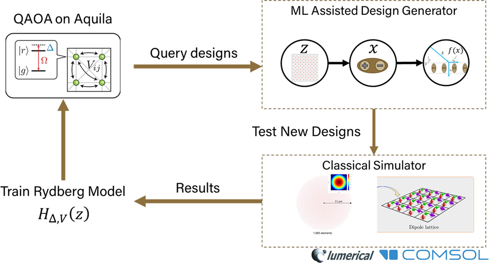
Recent developments in the field of quantum computing have shown that quantum annealers can offer practical advantages for global optimization and sampling in the latent space of binary variational autoencoders (bVAE) [1]. Considering these advances, we propose an extension to the bVAE-QUBO algorithm that utilizes Rydberg atoms in a Bayesian informed optimization algorithm [2].
In our proposed framework, we develop a novel machine learning optimization framework that preserves the Rydberg interaction and uses a Bayesian optimization approach for global optimization with Rydberg atoms and Quantum Approximate Optimization Algorithm (QAOA) [3].
The proposed framework leverages the strengths of Rydberg atom systems in quantum computing and the potential of QAOA for solving optimization problems. By combining these two approaches, we hope to develop a powerful tool for engineering applications that require efficient global optimization.
References:
[1] Wilson et al. Applied Physics Reviews 8, 041418 (2021); https://doi.org/10.1063/5.0060481
[2] Ebadi et al Nature, Volume 595, Issue 7866, p.227-232
[3] Farhi et al arXiv:1411.4028 [quant-ph]
Diffusion Modeling for Photonics
Project Team: Blake Wilson, Michael Bezick
The field of photonics has witnessed a tremendous growth in recent years, and the ability to learn statistical distributions in this domain is essential for applications such as photonic chip design, optical communication, and sensing. Inspired by the success of diffusion modeling in image generation tasks like DALL-E [1,2], we propose the use of diffusion models for learning statistical distributions in photonics. The proposed framework involves training a diffusion model to generate samples from a given distribution by iteratively applying a sequence of diffusion steps. The diffusion steps introduce a noise vector to the data and progressively reduce its variance, resulting in a sample from the desired distribution. We aim to use this framework to learn complex statistical distributions of photonics such as light scattering patterns, spectral properties, and temporal dynamics of photonic systems.
The proposed diffusion model will be evaluated on benchmark problems in photonics, such as image reconstruction and sensing. We will compare the performance of our framework with existing machine learning approaches such as convolutional neural networks and principal component analysis to demonstrate its potential advantages. The results of this project have the potential to provide a new tool for learning statistical distributions in photonics and to offer insights into the performance of diffusion modeling in this field. This may pave the way for future research on the practical applications of diffusion modeling in photonics, such as photonic device design and optimization, and may have implications for the broader field of machine learning.
References:
[1] Sohl-Dickstein et al arXiv:1503.03585 [cs.LG]
[2] Ramesh et al arXiv:2102.12092 [cs.CV]
Plasmonic Color Printing
Project Team: Sarah N. Chowdhury, Jeffrey Simon, Michal P. Nowak, Ludmila J. Prokopeva, Karthik Pagadala, Colton Fruhling, Piotr Nyga, Esteban Garcia Bravo
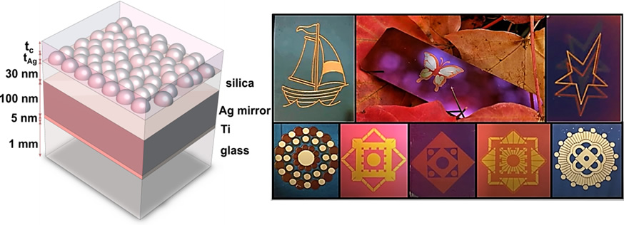
Plasmonic colors is a fade-free and environment-friendly method of color generation using metals like silver and dielectrics like silica which are abundant in nature. Our technique utilizes the idea of incorporating semicontinuous metal films (SMF) (tAg), which are randomly distributed metal nanoparticles and a laser as the means for generation of colors. Upon illumination of light, electromagnetic energy is concentrated around these metal nanoparticles in regions known as ‘hotspots’ where the local fields are significantly intensified compared to the incident light. This results in strongly enhanced nonlinear responses and other interesting optical phenomena. SMFs are then deposited on a metallic (Ag) mirror with a sub-wavelength-thick dielectric (SiO2) to utilize the gap-plasmon modes and observe colors in the reflection mode. A focused laser beam when impinged can locally modify, reshape, sinister and fragment the shapes and geometries of these nanoparticles through thermal heating of metallic nanostructures in the vicinity of these hotspots. As a result of such local photomodification, spectrally and polarization selective changes occur in the scattering, transmittance, reflectance and absorption spectra due to the gradual structural modifications, occurring in the nanometer-scale areas. This results in a wide range of non-fading color gamut from blue to green, red, and yellow. This process of laser printing modifies the nanoparticles to generate different colors without posing the threat of inhalation of such particles.
References:
[1] S. N. Chowdhury, L. Prokopeva, S. Peana, P. Nyga, E. Bravo, A. V. Kildishev, V. M. Shalaev, and A. Boltasseva, “Plasmonic Color Printing with Semicontinuous Silver Films and Modeling of Inhomogeneous Broadening”, in Bulletin of the American Physical Society, (American Physical Society, 2022), W12. 00007.
[2] S. N. Chowdhury, P. Nyga, Z. A. Kudyshev, E. Garcia Bravo, A. S. Lagutchev, A. V. Kildishev, V. M. Shalaev, and A. Boltasseva, "Lithography-Free Plasmonic Color Printing with Femtosecond Laser on Semicontinuous Silver Films," ACS Photonics 8, 521–530 (2021).
[3] S. N. Chowdhury, P. Nyga, Z. Kudyshev, E. Garcia, A. V. Kildishev, V. M. Shalaev, and A. Boltasseva, "Non-Fading Plasmonic Color Printing on Semicontinuous Metal Films with Protective Atomic Layer Deposition," in Conference on Lasers and Electro-Optics (Institute of Electrical and Electronics Engineers Inc., 2020), p. SF2R.2.
[4] P. Nyga, S. N. Chowdhury, Z. Kudyshev, M. D. Thoreson, A. V. Kildishev, V. M. Shalaev, and A. Boltasseva, "Laser-induced color printing on semicontinuous silver films: red, green and blue," Opt. Mater. Express 9, 1528 (2019).
Meta-Cavity-Mediated Strong Light-Matter Coupling in Two-Dimensional Materials
Project Team: Omer Yesilyurt, Karthik Pagadala, Vahagn Mkhitaryan
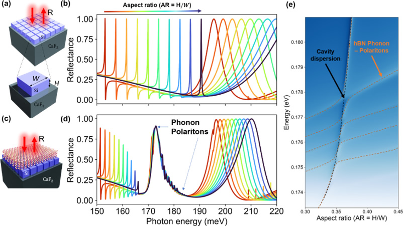
Figure: Simple metamaterial cavity design for preliminary simulations. Panels (a) and (b) show the schematics of the meta-cavity (a) used in the simulations and the reflection coefficient (b) at normal incidence depending on the incidence photon energy. The curves with different colors in panel (b) correspond to the same metamaterial but with different geometrical aspect-ratio defined as AR = H/W, for fixed cube height H = 1 um and for aspect-ratio ranging from 0.3 to 0.4. Panels (c) and (d) are respectively the schematics and the reflectance of the same cavity but with 30 nm thick hBN layer on it which supports phonon-polaritons. Panel (e) shows the dispersion diagram of the combined system where the clear anti-crossings are seen due to hybridization of the metamaterial cavity photons and the phonon polaritons in hBN.
Brief Project Descripton:
Plasmonic colors is a fade-free and environment-friendly method of color generation using metals like silver and dielectrics like silica which are abundant in nature. Our technique utilizes the idea of incorporating semicontinuous metal films (SMF) (tAg), which are randomly distributed metal nanoparticles and a laser as the means for generation of colors. Upon illumination of light, electromagnetic energy is concentrated around these metal nanoparticles in regions known as ‘hotspots’ where the local fields are significantly intensified compared to the incident light. This results in strongly enhanced nonlinear responses and other interesting optical phenomena. SMFs are then deposited on a metallic (Ag) mirror with a sub-wavelength-thick dielectric (SiO2) to utilize the gap-plasmon modes and observe colors in the reflection mode. A focused laser beam when impinged can locally modify, reshape, sinister and fragment the shapes and geometries of these nanoparticles through thermal heating of metallic nanostructures in the vicinity of these hotspots. As a result of such local photomodification, spectrally and polarization selective changes occur in the scattering, transmittance, reflectance and absorption spectra due to the gradual structural modifications, occurring in the nanometer-scale areas. This results in a wide range of non-fading color gamut from blue to green, red, and yellow. This process of laser printing modifies the nanoparticles to generate different colors without posing the threat of inhalation of such particles.
References:
[1] S. N. Chowdhury, L. Prokopeva, S. Peana, P. Nyga, E. Bravo, A. V. Kildishev, V. M. Shalaev, and A. Boltasseva, “Plasmonic Color Printing with Semicontinuous Silver Films and Modeling of Inhomogeneous Broadening”, in Bulletin of the American Physical Society, (American Physical Society, 2022), W12. 00007.
[2] S. N. Chowdhury, P. Nyga, Z. A. Kudyshev, E. Garcia Bravo, A. S. Lagutchev, A. V. Kildishev, V. M. Shalaev, and A. Boltasseva, "Lithography-Free Plasmonic Color Printing with Femtosecond Laser on Semicontinuous Silver Films," ACS Photonics 8, 521–530 (2021).
[3] S. N. Chowdhury, P. Nyga, Z. Kudyshev, E. Garcia, A. V. Kildishev, V. M. Shalaev, and A. Boltasseva, "Non-Fading Plasmonic Color Printing on Semicontinuous Metal Films with Protective Atomic Layer Deposition," in Conference on Lasers and Electro-Optics (Institute of Electrical and Electronics Engineers Inc., 2020), p. SF2R.2.
[4] P. Nyga, S. N. Chowdhury, Z. Kudyshev, M. D. Thoreson, A. V. Kildishev, V. M. Shalaev, and A. Boltasseva, "Laser-induced color printing on semicontinuous silver films: red, green and blue," Opt. Mater. Express 9, 1528 (2019).
Thermophotovoltaic Energy Conversion using Machine-Learning-Optimized Refractory Metasurfaces
Project Team: Zelong Ding, Karthik Pagadala, Omer Yesilyurt, Yuheng Chen
Project Descripton:
Efficient thermophotovoltaic (TPV) systems that convert heat into electricity are envisioned to play a crucial role in the emerging sustainable economy. Realizing high-efficiency systems for thermal energy conversion requires both advancing fundamental knowledge of photonic design, materials and fabrication approaches. There is a critical need for complex and multiparameter optimization of both advanced multi-functional design components and their constituent material platforms that are stable against the harsh environment and extreme temperatures. This project will merge the optical properties of Titanium Nitride with advanced optimization of the TPV designs to realize highly efficient conversion of heat to electrical energy. The major goals are to create a fundamentally new optimization framework for realization of advanced TPV components and, specifically, to 1) advance topology optimization via machine-learning algorithms; 2) expand the optimization parameter space into materials domain through the development of tailorable optical materials database; and 3) integrate machine-learning based analysis with photonic designs tailored for TPV applications.
Project References:
Z. A. Kudyshev, A. V. Kildishev, V. M. Shalaev, and A. Boltasseva, “Machine learning–assisted global optimization of photonic devices,” Nanophotonics Nanophotonics 10 (1), 371–383 (2021)
W. Ma, Z. Liu, Z. A. Kudyshev, A. Boltasseva, W. Cai, Y. Liu, “Deep learning for the design of photonic structures,” Nature Photonics 15, 77–90 (2021)
H. Reddy and V. M. Shalaev, Plasmonic hot-carriers and their applications: opinion, Opt. Mat. Expr., v. 11, pp. 3827-3832 (2021)
H. Reddy, U. Guler, Z. Kudyshev, A. V. Kildishev, V. M. Shalaev, and A. Boltasseva, “Temperature-Dependent Optical Properties of Plasmonic Titanium Nitride Thin Films,” ACS Photonics, vol. 4, no. 6, pp. 1413–1420, Jun. 2017, doi: 10.1021/acsphotonics.7b00127.
All-optical modulation with single-photons using electron avalanche
Project Team: Demid Sychev (Lead), Peigang Chen
Project Descripton:
In this research we’re planning to investigate new principles for ultrafast light detection light. Current limitation for light quantum technologies is connected to limited ability of photodetectors to work in ultrafast regime – single photon detectors have long dead time(~10-40ns), photodetection of light in continues variables is limited by bandwidth of a few GHz. These limitations constrain the scalability of modern quantum photonic technologies, because of the finite coherence times.
In the presented proposal we suggest to use optical beam for probing an avalanche caused by single photon in silicon semiconductor heterostructure. Conventional single photon avalanche detectors(SPAD) use the effect of current multiplication to amplify weak signal of a single photon, what makes this kind of the detector very sensitive. The opposite side of the coin is that SPADs are getting blind for several nanoseconds after the event. Because of the principle of detection, which involves detection of a current by electronics, the dead time interval can’t be less then several ns [1].
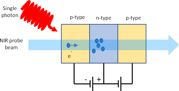 Schematics of the proposed device
In Ref. [1] we suggest to suppress avalanche immediately after the occurrence by specially designed p-n-p heterosctucture as presented in the figure. Incident photon comes from the left side and excite an electron in region, dopped by holes(p-type). Moving to the first p-n transition it causes electron multiplication in a thin n-type region under the influence of applied voltage. Then, due to the drift, avalanche achieves right region with high concentration of holes, in which it is suppressed due to processes of electron-hole recombination. Because of early suppression given type of avalanche can’t be detected by electronics. Nevertheless, its detection can be done with near-infrared radiation, which will “feel” modulation of electron’s density in the layer and do not cause excitation of an electron because of low photon energy. Modulation of the probe light in its turn can be detected by well-established ultrafast method of nonlinear optics[2]. Potentially, such a device could detect single photons with >90% quantum efficiency with less than 10ps dead time.
Project References:
[1] Alessandro Spinelli and Andrea L. Lacaita, IEEE TRANSACTIONS ON ELECTRON DEVICES, 44, 11(1997)
[2] P. Ryczkowski et. al., Nature Photonics 12, 221(2018)
MW-Optical Frequency Conversion
Project Lead: Demid Sychev
Collaborators: Yong Chen, Alex Ma, Pramey Upadhyaya
In this project we will try to realize a frequency conversion of a single photon from a microwave (MW) frequency range to optical. Similar to [1], in this idea we will realize strong coupling regime between MW and spin defects in hBN by placing hBN flake inside a MW cavity and measuring optical and MW signal from a sample. In contrast to previously reported works, we’re planning to use emitters in hBN instead of NV centers in diamond.
This challenging work requires very low temperatures (<100mK), equipment on both parts of the spectra (MW and optical) to detect the desired effect. It assumes a close collaboration between our group, Yong Chen, Alex Ma and Pramey. As a part of this project, currently we are building optical set-up around a mK cryostat (photo below).
References:
[1] Y. Kubo et. al. Phys. Rev. Lett. 105, 140502 (2010)
Novel Photonic Materials
Project Contact: Colton Fruhling
There is an ever-increasing desire discover understand and fabricate novel materials for optical and photonics. In this project, we study multiple new materials to gain control over their properties and utilize them for photonic devices. Three of the main categories explored are (1) metal nitrides such as titanium nitride, zirconium nitride, and hafnium nitride, (2) transparent conducting oxides like aluminum zinc oxide, gallium zinc oxide, and cadmium oxide and (3) the recent expansive family of MXenes.
The optical properties of these materials can be controlled by fabrication parameters such as thickness for titanium nitride and zinc oxide [???]. Another important critical tuning know is the relative proportions of constituents such as doping materials and concentration in zinc oxides [???] and transition metals in MXenes. The resulting understandings from these studies have been employed for a wide range of photonic applications like Ferrell-Berreman mode absorbers composed of … and broadband absorbing MXene metasurfaces. They have also been used to build controllable plasmonic metasurfaces for enhancing nonlinear coupling. Many of these materials also possess ultrafast optical responses desirable for applications such as optical switching. In a recent study, we have combined multiple of these novel materials to fabricate designer temporal optical response [???].
References:
[1] Wang, Z. et al. Dynamically controlled random lasing with colloidal titanium carbide MXene. Opt. Mater. Express, OME 10, 2304–2312 (2020).
[2] Chaudhuri, K. et al. Highly Broadband Absorber Using Plasmonic Titanium Carbide (MXene). ACS Photonics 5, 1115–1122 (2018).
[3] Khurgin, J. B. et al. Adiabatic frequency shifting in epsilon-near-zero materials: the role of group velocity. Optica, OPTICA 7, 226–231 (2020).
[4] Carnemolla, E. G. et al. Degenerate optical nonlinear enhancement in epsilon-near-zero transparent conducting oxides. Opt. Mater. Express, OME 8, 3392–3400 (2018).
[5] Kim, J. et al. Dynamic Control of Nanocavities with Tunable Metal Oxides. Nano Lett. 18, 740–746 (2018).
[6] Bruno, V. et al. Dynamical Control of Broadband Coherent Absorption in ENZ Films. Micromachines 11, 110 (2020).
[7] Saha, S. et al. Engineering the Temporal Dynamics with ‘Fast’ and ‘Slow’ Materials for All-Optical Switching. (CANT FIND THE OFFICIAL PUBLISH VERSION OF THIS, IS IT STILL PENDING?)
[8] Kinsey, N., DeVault, C., Boltasseva, A. & Shalaev, V. M. Near-zero-index materials for photonics. Nat Rev Mater 4, 742–760 (2019).
[9] Jaffray, W. et al. Near-zero-index ultra-fast pulse characterization. Nat Commun 13, 1–8 (2022).
[10] Stockman, M. I. et al. Roadmap on plasmonics. J. Opt. 20, 043001 (2018).
[11] Saha, S. et al. Tailoring the Thickness‐Dependent Optical Properties of Conducting Nitrides and Oxides for Epsilon‐Near‐Zero‐Enhanced Photonic Applications. Advanced Materials 2109546 (2022) doi:10.1002/adma.202109546.
[12] Jaffray, W., Saha, S., Shalaev, V. M., Boltasseva, A. & Ferrera, M. Transparent conducting oxides: from all-dielectric plasmonics to a new paradigm in integrated photonics. Adv. Opt. Photon., AOP 14, 148–208 (2022).
[13] Kudyshev, Z. A., Kildishev, A. V., Boltasseva, A. & Shalaev, V. M. Tuning Topology of Photonic Systems with Transparent Conducting Oxides. ACS Photonics 6, 1922–1930 (2019).
[14] Fruhling, C., Ozlu, M. G., Saha, S., Boltasseva, A. & Shalaev, V. M. Understanding all-optical switching at the epsilon-near-zero point: a tutorial review. Appl. Phys. B 128, 1–12 (2022).
[15] Carnemolla, E. G. et al. Visible photon generation via four-wave mixing in near-infrared near-zero-index thin films. Opt. Lett., OL 46, 5433–5436 (2021).
[16] Korobenko, A. et al. High-harmonic generation in metallic titanium nitride. Nat Commun 12, 1–6 (2021).
Diamond Color Centers as Single Photon Sources
Project Team: Zach Martin, Demid Sychev, Peigang Chen
Color centers in diamond are one of the most extensively studied categories of single photon sources with high brightness, great scalability, as well as the capability to form spin-photon interfaces for quantum memories and quantum sensing. They have been investigated in both bulk diamond and diamond nanoparticles (nanodiamonds or NDs). Compared to bulk diamond, nanodiamonds containing color centers possess some attractive properties: The small dimensions of NDs enable effective coupling of color centers with photonic modes, which can be challenging for color centers in bulk diamond; Using the recently developed pick-and-place techniques, color centers in nanodimoands with desired optical properties could be deterministically relocated and placed onto photonic/plasmonic structures for quantum emission engineering. We are exploring the effective fabrication of single color centers, including silicon vavancy (SiV) and germanium vavancy (GeV) centers, in sub-50 nm NDs, as well as their integration with nanoscale plasmonic cavities and hybrid plasmonic-dielectric resonators that can provide high Purcell factors. This promises ultrafast single photon emission of on-demand indistinguishable photons at cryo-free temperatures.
References:
X. Xu, Z. O. Martin, M. Titze, Y. Wang, D. Sychev, J. Henshaw, A. S. Lagutchev, H. Htoon, E. S. Bielejec, S. I. Bogdanov, V. M. Shalaev, A. Boltasseva, Fabrication of single color centers in sub-50 nm nanodiamonds using ion implantation, Nanophotonics, 2023, 12, 3, 485–494.
S. I. Bogdanov, O. A. Makarova, X. Xu, Z. O. Martin, A. S. Lagutchev, M. Olinde, D. Shah, S. N. Chowdhury, A. R. Gabidullin, I. A. Ryzhikov, I. A. Rodionov, A.V. Kildishev, S. I. Bozhevolnyi, A. Boltasseva, V. M. Shalaev, J. B. Khurgin, Ultrafast quantum photonics enabled by coupling plasmonic nanocavities to strongly radiative antennas, Optica, 2020, 7, 5, 463–469.
Chin‐Cheng Chiang, Simeon I Bogdanov, Oksana A Makarova, Xiaohui Xu, Soham Saha, Deesha Shah, Zachariah O Martin, Di Wang, Alexei S Lagutchev, Alexander V Kildishev, Alexandra Boltasseva, Vladimir M Shalaev, Chip‐Compatible Quantum Plasmonic Launcher, Adv. Opt. Mater., 2020, 8, 20, 2000889.
Engineering Quantum Emitters in 2D Hexagonal Boron Nitride – Fabrication, Enhancement and Integration
Project Lead: Brandon Triplett
Project Team: Abhishek Solanki, Brandon Triplett, Demid Sychev, Zach Martin, Jeffrey Simon, Morris Yang
Two-dimensional hexagonal boron nitride (hBN) is receiving increasing attention in quantum optics/photonics as it hosts quantum emitters that are promising for quantum computing, quantum sensing, etc. In one project, we developed a radiation- and lithography-free route to deterministically create single-photon emitters (SPEs) in hBN by nanoindentation with an atomic force microscopy. The method applies to hBN on flat, chip-compatible silicon-based substrates, and we achieved an SPE yield of up to 36%. With this technique, we aim to explore the deterministic, optimized integration of hBN SPEs with photonic and plasmonic devices as a way to tailor/improve the optical properties of such emitters. One important goal is to obtain indistinguishable photons from hBN SPEs that are strongly enhanced in a plasmonic cavity, which hold great potential for quantum computing, quantum communication, etc.
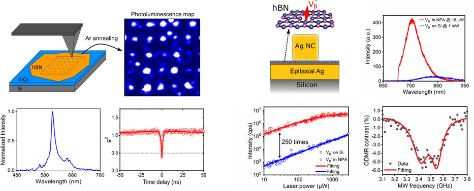
In another project, we study the recently discovered negatively charged boron vacancy (VB-) defect hBN. VB- is optically active and possesses spin properties that are suitable for sensing at extreme scales. One limitation of VB- defects is their low quantum yield or low brightness. To resolve this issue, we couple them with optimized plasmonic nanocavity structures and have realized emission intensity enhancement of 250 times, nearly an order of magnitude higher than previous reports. Our achievements pave the way for the practical integration of VB- defects for quantum sensing. With the strong Purcell enhancement, our next step is to explore the isolation of single VB- defects, which can further expand their application in the field of quantum information technologies.
References:
X. Xu, A. B. Solanki, D. Sychev, X. Gao, S. Peana, A. S. Baburin, K. Pagadala, Z. O. Martin, S. N. Chowdhury, Y. P. Chen, T.Taniguchi, K. Watanabe, I. A. Rodionov, A. V. Kildishev, T. Li, P. Upadhyaya, A. Boltasseva, V. M. Shalaev, Greatly Enhanced Emission from Spin Defects in Hexagonal Boron Nitride Enabled by a Low-Loss Plasmonic Nanocavity, Nano Lett. 2023, 23, 1, 25–33.
X. Xu, Z. O. Martin, D. Sychev, A. S. Lagutchev, Y. P. Chen, T. Taniguchi, K. Watanabe, V. M. Shalaev, A. Boltasseva, Creating quantum emitters in hexagonal boron nitride deterministically on chip-compatible substrates, Nano Lett. 2021, 21, 19, 8182–8189.
X. Xu, A. B. Solanki, D. Sychev, X. Gao, S. Peana, A. S. Baburin, K. Pagadala, Z. O. Martin, S. N. Chowdhury, Y. P. Chen, T.Taniguchi, K. Watanabe, I. A. Rodionov, A. V. Kildishev, T. Li, P. Upadhyaya, A. Boltasseva, V. M. Shalaev, “Greatly Enhanced Emission from Spin Defects in Hexagonal Boron Nitride Enabled by a Low-Loss Plasmonic Nanocavity,” in Bulletin of the American Physical Society, 2023.
X. Xu, A. B. Solanki, D. Sychev, X. Gao, Z. O. Martin, A. S. Baburin, Y. P. Chen, I. A. Rodionov, A. Kildishev, T. Li, P. Upadhyaya, A. Boltasseva, V. M. Shalaev, “Plasmon-enhanced Quantum Emission from Spin Defects in Two-dimensional Hexagonal Boron Nitride,” in 2022 Conference on Lasers and Electro-Optics (CLEO).
X. Xu, Z. O. Martin, D. Sychev, A. S. Lagutchev, Y. P. Chen, T. Taniguchi, K. Watanabe, V. M. Shalaev, A. Boltasseva, “Deterministically Creating Single-Photon Emitters in Hexagonal Boron Nitrides on Chip-Compatible Substrates,” in APS March Meeting 2022.
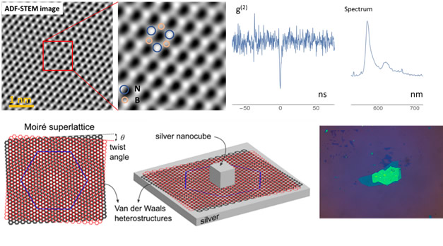
Enhanced Single Photon Emission from hBN Using a Plasmonically-Enhanced Femtosecond Pulsed Laser
Project Lead: Brandon Triplett
Project Team: Abhishek Solanki, Brandon Triplett, Demid Sychev, Zach Martin, Jeffrey Simon, Morris Yang
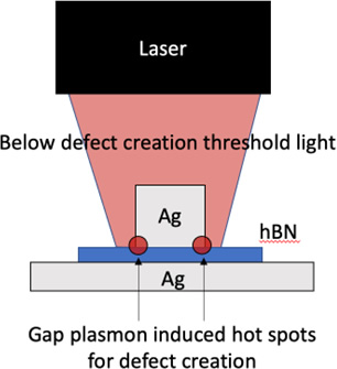
Single photon emitters in hexagonal boron nitride (hBN) are a promising platform for quantum technologies, such as quantum communication, computing, and sensing, due to its unique opto-electrical properties, mechanical robustness, and its ability to host spin defects. In this project, we aim to create efficient sources of single photons by using a femtosecond pulsed laser to induce defects in the hBN lattice, specifically the boron vacancy spin defect. We plan to enhance the efficiency of these single photon emitters by encapsulating thin hBN layers in a silver nanocube and metallic layer cavity that utilizes a plasmonic structure to generate a gap plasmon, which enhances the femtosecond laser pulse at a certain position in the cavity with the intent to localize the creation of the spin defects. We anticipate that the same cavity structure will also plasmonically enhance the outcoupling of the single photons, further improving their efficiency. This research has the potential to advance our understanding of hBN-based quantum technologies and bring us closer to practical applications of these technologies.
References:
Gao, Xingyu, et al. “Femtosecond Laser Writing of Spin Defects in Hexagonal Boron Nitride.” ACS Photonics, vol. 8, no. 4, 2021, pp. 994–1000., https://doi.org/10.1021/acsphotonics.0c01847.
Indistinguishable Single Photons at Telecom Wavelengths in NVs through SPDC
Project Lead: Morris Yang
Project Team: Demid Sychev, Peigang Chen, Pranshu Maan
Beyond bare quantum dots and conventional NVs, NVs’ emission can be enhanced with dielectric and plasmonic cavities to help raise the temperature limits. Although NVs don’t possess high coherence times for optical levels among emitters - thus not allowing natural generation of indistinguishable photons at higher temperatures - they have the best spin properties. NV centers in nanodiamonds serve as good single photon sources because they generate stable, broadband, and anti-bunched emission. In our proposal, we will apply time and frequency conversion for photons emitted from plasmonically enhanced NVs to generate single photons with high indistinguishability. We will send the photons (637nm) from NVs and an auxiliary pump pulse into a nonlinear (NL) crystal, whereby through difference frequency generation the output photons will be limited in frequency and time. The photons will be Fourier-transform limited – centering around a single wavelength (1260nm) – satisfying the conditions necessary for indistinguishability at higher temperatures. Compared to previously implemented experiments, our idea gives control not only over the wavelength but also the temporal shape of a photon. Moreover, the output photon will be in near-infrared range, which is beneficial for long-range communication. Crucially, NVs has optical transitions and spin; entanglement between photons can be converted to entanglement between spins which is the essential procedure for building future quantum networks. By taking advantage of the increased collection frequency in nanodiamonds and increased emission rate when coupled to, plasmonically enhanced NVs in nanodiamonds will serve as reliable source of indistinguishable single photon. The optical setup will be built using NL crystals and an interferometer for verification. The produced indistinguishable photon can be entangled and encoded in horizontal and vertical polarizations after certain transformation.
Optically Active Spin Defects in Aluminum Nitride by Ion Implantation
Project Team: Alexander Senichev, Zachariah Martin, in collaboration with Los Alamos National Laboratory's' Han Htoon and Yongqiang Wang
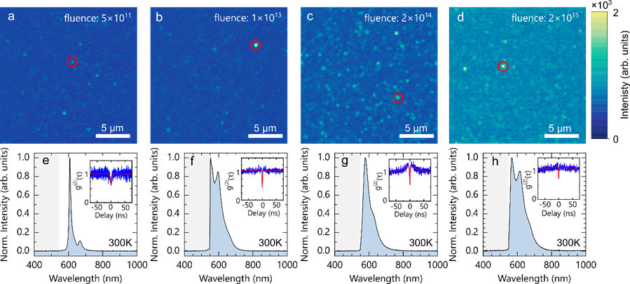
Aluminum nitride (AlN) is a promising material platform for integrated quantum photonic technologies. First-principles calculations have shown that transition-metal impurities, such as Ti and Zr, can form stable complexes with nitrogen vacancies resulting in defects possessing a high-spin ground state [1] [2].
We study the generation of single-photon emitters in AlN through implantation of Zr ions, which were theoretically predicted to exhibit spin properties. First, we used a broad beam ion implantation to determine the implantation energy, fluence, and post-implantation procedures required to generate single-photon emitters. Specifically, we prepared a series of samples using a different Zr ion implantation fluences Φ_Zr to study their impact on emitter formation and employed thermal annealing to activate emitters. We demonstrated the formation of single-photon emitters in Zr-implanted samples after thermal annealing confirmed by photoluminescence intensity maps and second-order autocorrelation measurements. Importantly, the density of isolated emitters was found to increase with greater implantation fluence [3].
Current work is focused on revealing the defect structure responsible for single-photon emission in Zr- implanted AlN and addressing their spin properties.
[1] J. B. Varley, A. Janotti, and C. G. Van De Walle, Defects in AlN as Candidates for Solid-State Qubits, Phys. Rev. B 93, 161201 (2016).
[2] H. Seo, M. Govoni, and G. Galli, Design of Defect Spins in Piezoelectric Aluminum Nitride for Solid-State Hybrid Quantum Technologies, Sci. Rep. 6, 20803 (2016).
[3] A. Senichev, Z. O. Martin, Y. Wang, H. Htoon, A. S. Lagutchev, A. Boltasseva, and V. M. Shalaev, Single-Photon Emitters in Aluminum Nitride by Zr Ion Implantation, in CLEO (2023), p. FTh1E.2.
Time-Frequency Conversion of Single Photons
Project Lead: Demid Sychev
Project Team: Peigang Chen, Pranshu Maan
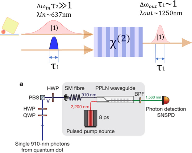
Solid-state quantum emitters (QEs) are key elements of future quantum communication, information processing and quantum sensing technologies as sources of single photons. Nitrogen vacancies (NVs) in diamond have recently emerged as promising candidates to enable on-chip, room-temperature single photon emitters. To-date, applicability of NVs for building larger quantum systems with several qubits operating at liquid nitrogen temperatures has however been limited due to NV’s relatively poor optical properties. In particular, huge dephasing rate of NVs due to interaction with phonons lead to a poor photon’s quality, which cannot be used for observing multiphoton entanglement and, as a consequence, to be used for transferring quantum information between several solid state emitters. To avoid these effects, people are applying cryogenic temperature in combination with photonic cavities, which is usually still not enough to observe high-quality indistinguishable single photon at high temperatures. These factors hinder the development of NV-based scalable quantum devices and systems for future quantum sensing, quantum communications and computing.
Here, we are trying to overcome these limitations by improving the optical properties of a single photons emitted from NV center through a non-linear optical time-frequency conversion. Single photons from an NV center are sent to a non-linear optical crystal with an ancilla optical beam. Due to phase-matching conditions and time duration of an ancilla laser pulse, the output single photon is expected to have a certain frequency and temporal characteristics, which eventually allows significantly improving the quality of an output photon and make them indistinguishable in frequency-time domain. Moreover, the approach allow shifting the central frequency of a photons from visible to near-infrared range(NIR), which makes it more practical for quantum networks due to lower optical losses in NIR range.
References:
[1] De Greve, K., Yu, L., McMahon, P. et al. Nature 491, 421–425 (2012).
Deterministic Fabrication and Integration of Single Photon Emitters in SiN/SiO2
Project Team: Samuel Peana, Omer Yesilyurt, Vahagn Mkhitaryan, Alexander Senichev, Zachariah Martin
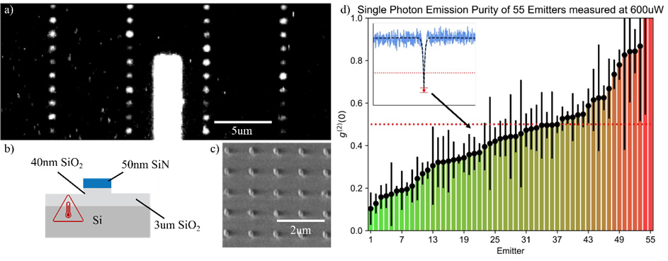
Recently bright and stable native single photon emitters were discovered in Silicon Nitride (SiN). Such native emitters allow for the monolithic integration of emitters into industry standard SiN photonic circuits without many of the difficulties associated with hybrid integration such as: fabrication complexity and poor light coupling [1-4]. We build on this discovery by demonstrating a large-scale high yield fabrication method for these emitters. By nanostructuring SiN on SiO into nanopillars followed by thermal annealing it was found that approximately 67% of the emitters demonstrate single photon emission.
This method of fabrication is capable of producing industrial quantities of single photon emitters. Furthermore, this method allows for the lithographic definition of these emitters with relatively high spatial accuracy. Finally, the emitters being patterned are native to silicon nitride avoiding many of the issues associated with hybrid integration. These three features promise to pave the way towards quantum photonic systems deterministically and seamlessly integrated with large numbers of single photon emitters. Current efforts are directed towards the integration of such emitters with nanophotonic devices and further refinement of this process to enhance yields and emitter quality.
References:
S. Peana, O. Yesilyurt, A. Senichev, Z. O. Martin, V. Mkhitaryan, A. S. Lagutchev, A. Boltasseva, and V. M. Shalaev, "Large Scale Site-Controlled Fabrication of Single Photon Emitters in Silicon Nitride Nanopillars," in Frontiers in Optics + Laser Science 2022 (FIO, LS), Technical Digest Series (Optica Publishing Group, 2022), paper FTh3E.1.
S. Peana, O. Yesilyurt, V. Mkhitaryan, A. Senichev, Z. O. Martin, A. S. Lagutchev, A. Boltasseva, and V. M. Shalaev, "Large Scale Deterministic Creation of Single Photon Emitters in Silicon Nitride Nanopillars," in Conference on Lasers and Electro-Optics, Technical Digest Series (Optica Publishing Group, 2022), paper FS4B.5.
Senichev, A., Peana, S., Martin, Z.O., Yesilyurt, O., Sychev, D., Lagutchev, A.S., Boltasseva, A. and Shalaev, V.M., 2022. Silicon nitride waveguides with intrinsic single-photon emitters for integrated quantum photonics. ACS Photonics, 9(10), pp.3357-3365.
Senichev, A., Martin, Z.O., Peana, S., Sychev, D., Xu, X., Lagutchev, A.S., Boltasseva, A. and Shalaev, V.M., 2021. Room-temperature single-photon emitters in silicon nitride. Science Advances, 7(50), p.eabj0627.
Electrically driven single-photon sources in silicon nitride
Project Team: Alexander Senichev, Zachariah Martin, Artem Kryvobock
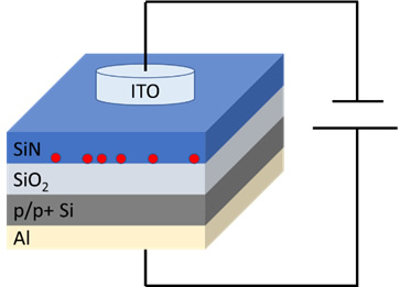
This project focuses on the development of compact room-temperature electrically driven single-photon sources in wide-bandgap semiconductors, which would enable scalable on-chip generation of quantum states of light without external optical excitation of color centers [1] [2]. Intrinsic single-photon emitters in SiN is a promising material platform for the realization of single-photon electroluminescence with a potential for a variety of quantum photonic application.
References:
[1] A. Lohrmann, N. Iwamoto, Z. Bodrog, S. Castelletto, T. Ohshima, T. J. Karle, A. Gali, S. Prawer, J. C. McCallum, and B. C. Johnson, Single-Photon Emitting Diode in Silicon Carbide, Nat. Commun. 6, (2015).
[2] X. Lin, X. Dai, C. Pu, Y. Deng, Y. Niu, L. Tong, W. Fang, Y. Jin, and X. Peng, Electrically-Driven Single-Photon Sources Based on Colloidal Quantum Dots with near-Optimal Antibunching at Room Temperature, Nat. Commun. 8, 1 (2017).
Low Temperature Studies of Quantum Emitters in SiN
Project Team: Zach Martin, Alexander Senichev, Samuel Peana, Benjamin Lawrie (ORNL)
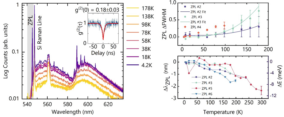
Our recent discovery of intrinsic single-photon emitters (SPEs) in silicon nitride (SiN) has attracted substantial interest for applications in integrated quantum photonics because of their high single-photon purity at room temperature [1] and because of their integrability into technologically mature SiN photonic devices [2]. For this project, we are studying the optical transition wavelengths, linewidths, and antibunching of these emitters as a function of temperature down to 4.2K. So far, we have found the emergence of narrow emission lines at cryogenic temperatures; the linewidths of these narrow peaks at 4.2K are mainly determined by spectral diffusion as evidenced by their Gaussian shape. Time-resolved spectral measurements allow us to resolve the spectral diffusion of peaks with instrument-limited linewidths.
This is a promising development, though quantifying the indistinguishability of these emitters beyond the instrument limit will require photoluminescence excitation spectroscopy (PLE) or Hong-Ou-Mandel (HOM) interferometry. The current tasks for this project are therefore to construct a PLE and HOM measurement setup with our collaborators at Oak Ridge National Laboratory to show indistinguishable photon generation from SiN SPEs at low temperatures. In addition to their technological applications, the low temperature PL spectra have revealed a rich structure. It is our hope that these low temperature measurements in conjunction with materials studies and theoretical modeling can also shed light on the SPE defect structure and formation mechanisms.
References:
[1] A. Senichev et al., Sci. Adv. 7 50 (2021)
[2] A. Senichev et al., ACS Phot. 9 3357-3365 (2022)
[3] S. Peana et al., Frontiers in Optics + Laser Science 2022 (FIO, LS), paper FTh3E.1.
Silicon-Nitride Quantum Photonics with Intrinsic Single-Photon Emitters
Project Team: Alexander Senichev, Zachariah O. Martin, Samuel Peana, Owen M. Matthiessen, Omer Yesilyurt, Miroslava Marinova
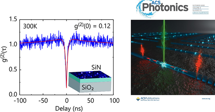
Silicon nitride (SiN) is one of the leading material platforms for quantum photonic integrated circuits (QPICs) offering ultralow optical losses, a broad transparency window, the absence of two-photon absorption in the telecommunication bands, a high refractive index, strong optical Kerr nonlinearity, and CMOS compatible and foundry friendly fabrication. Until recently, an intrinsic atomic-like source of single photons in SiN has been missing, which required hybrid heterogeneous integration with other materials that host quantum emitters. In our study, we discovered intrinsic single-photon emitters in SiN and established methods of their creation [1]. SiN quantum emitters exhibit high single-photon purity at room temperature and promise seamless integration with a technologically mature material platform [2].
The room-temperature operation, photoemission rate of up to 106 Hz, single-photon purity of g(2)(0)<0.2 without spectral filtering or background corrections, and stable emission make quantum emitters in SiN promising for applications in quantum communication protocols based on single-photon states such as quantum key distribution (QKD).
The ongoing work on intrinsic single-photon emitters in the SiN photonic platform is focused on in-depth studies of their photophysical properties [3] and improving key figures of merits required for applications in quantum information processing. We study the possibility of generating indistinguishable photons by introducing the plasmonic speed-up approach that may enable broader applications in quantum information technology.
References:
[1] A. Senichev, Z. O. Martin, S. Peana, D. Sychev, X. Xu, A. S. Lagutchev, A. Boltasseva, and V. M. Shalaev, Room-Temperature Single-Photon Emitters in Silicon Nitride, Sci. Adv. 7, FW4I.6 (2021).
[2] A. Senichev, S. Peana, Z. O. Martin, O. Yesilyurt, D. Sychev, A. S. Lagutchev, A. Boltasseva, and V. M. Shalaev, Silicon Nitride Waveguides with Intrinsic Single-Photon Emitters for Integrated Quantum Photonics, ACS Photonics 9, 3357 (2022).
[3] Z. O. Martin, A. Senichev, S. Peana, B. J. Lawrie, A. S. Lagutchev, A. Boltasseva, and V. M. Shalaev, Photophysics of Intrinsic Single-Photon Emitters in Silicon Nitride at Low Temperatures, ArXiv Prepr. 2301.10809, (2023).
Quantum Key Distribution with Solid-state Single-Photon Emitters
Project Team: Alexander Senichev, Zachariah Martin, Owen Matthiessen, Samuel Peana, Demid Sychev
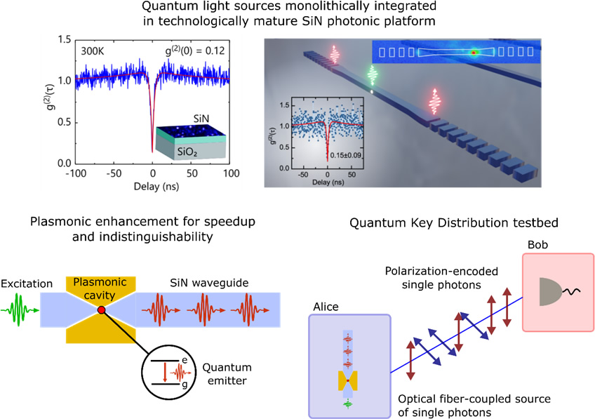
Solid-state single-photon emitters are particularly thought of for their application for quantum key distribution (QKD) due to their high efficiency compared to weak coherent laser pulses [1] [2]. Some of the QKD protocols, e.g., BB84, can use single photons prepared in different polarizations as polarization-encoded qubits, which do not require photon indistinguishability. Such QKD protocols require sources with (i) high efficiency, i.e. near unity probability to produce a single photon per a trigger pulse, (ii) high purity, i.e. low probability to emit more than one photon per pulse, as well as (iii) stable emission, (iv) operation at room temperature, and (v) high repetition frequencies. Brightness of >107 counts/s and photon purity of g(2)(0)<0.1 can be used as a benchmarks for emitters feasibility for QKD. Such performances can be achieved with intrinsic single photon emitters in silicon nitride (SiN) that have been discovered in our group. SiN quantum emitters are particularly interesting for QKD application due to the room-temperature operation, high single-photon purity up to g(2)(0)~0.08 and brightness ~106 Hz with the capability of monolithic integration with technologically important SiN photonic platform.
The project focuses on further improving SiN quantum emitters figures of merits required for real-world QKD applications. Specifically, the high repetition frequencies can be achieved by employing plasmonic enhancement of spontaneous emission. Moreover, plasmonic enhancement may allow emission speed-up to the level sufficient to overcome the rate of decoherence processes and generation of indistinguishable photons at non-cryogenic temperatures for applications in more complex quantum communication protocols. The brightness can be improved by using techniques for efficient collection of photons such as solid immersion lenses for far-field collection or topology-optimized waveguide couplers with subsequent direct outcoupling into optical fibers. Also, this project requires realization of testbed for evaluation of emitters for applications in QKD protocols, demonstration of particular protocols in the QKD setup, capability to switch and test different types of solid-state single-photon emitters.
References:
[1] M. Leifgen, T. Schröder, F. Gädeke, R. Riemann, V. Métillon, E. Neu, C. Hepp, C. Arend, C. Becher, K. Lauritsen, and O. Benson, Evaluation of Nitrogen- and Silicon-Vacancy Defect Centres as Single Photon Sources in Quantum Key Distribution, New J. Phys. 16, (2014).
[2] A. Al-Juboori, H. Z. J. Zeng, M. A. P. Nguyen, X. Ai, A. Laucht, A. Solntsev, M. Toth, R. Malaney, and I. Aharonovich, Quantum Key Distribution Using an Integrated Quantum Emitter in Hexagonal Boron Nitride, ArXiv Prepr. 2302.06212 1 (2023).
Nanolasing
Project Lead: Colton Fruhling
A primary goal in photonic research is the generation and control of light. In this project, we seek to achieve this goal in the extreme nanoscale world. Our research focuses on the design of nanoscale lasing cavities including those formed from photonic crystals [], plasmonics structures[], and unplanned random cavities []. We also explore lasing feedback mechanisms typically formed by the interference multiple resonances, which although they have energy enough to be considered free moving waves are nevertheless bound by the unique interference. These systems call bound states in the continuum can in principle possess infinite quality factors.
In addition to studying nanolasing cavities, we also explore novel materials for gain such as perovskites and exciting optical control materials like MXenes. In these systems we study the formation of feedback from unintentional random cavities which enjoy rich statistical and phase properties.
References:
S. Azzam et al, Dynamically Controlled Random Lasing with Colloidal Titanium Carbide MXene. OMEX (2020)
S. I. Azzam, J. Fang, J. Liu, Z. Wang, N. Arnold, T. A. Klar, L. J. Prokopeva, X. Meng, V. M. Shalaev, A. V. Kildishev, Exploring Time‐Resolved Multiphysics of Active Plasmonic Systems with Experiment‐Based Gain Models, Laser & Photonics Reviews, v. 13, no. 1 (2019): 1800071
S. I. Azzam, A. V. Kildishev, R. M. Ma, C. Z. Ning, R. Oulton, V. M. Shalaev, M. I. Stockman, J. L. Xu, and X. Zhang, Ten years of spasers and plasmonic nanolasers, Light: Science & Applications, v. 9, no. 1, pp. 1-21 (2020)
Azzam, S. I.; Kildishev, A. V. Photonic Bound States in the Continuum: From Basics to Applications. Advanced Optical Materials 2021, 9 (1), 2001469. https://doi.org/10.1002/adom.202001469.
Azzam, S. I.; Chaudhuri, K.; Lagutchev, A. S.; Jacob, Z.; Kim, Y. L.; Shalaev, V. M.; Boltasseva, A.; Kildishev, A. V. Single and Multi-Mode Directional Lasing from Arrays of Dielectric Nanoresonators. Laser and Photonics Reviews 2021, 15 (3). https://doi.org/10.1002/lpor.202000411.
Fruhling, C., Wang, K., Chowdhury, S., Xu, X., Simon, J., Kildishev, A., Dou, L., Meng, X., Boltasseva, A., Shalaev, V. M., Coherent Random Lasing in Subwavelength Quasi-2D Perovskites. Laser Photonics Rev 2023, 2200314. https://doi.org/10.1002/lpor.202200314
Nanolens Beam Homogenizer
Project Lead: Omer Yesilyurt
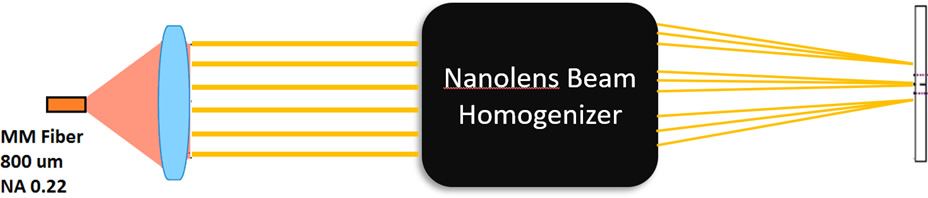
A beam homogenizer is an optical device that modifies a laser beam to create a flat-top beam with uniform optical intensity over a specific area, which is necessary for certain applications such as laser material processing and optical lithography. Beam homogenizers can generate square or circular intensity profiles and often use random or quasi-random changes to the beam's amplitude profile. Different types of beam homogenizers exist, including refractive and diffractive, but these often require expensive multi-level elements or strict dependence on entrance profile and alignment. Multi-aperture elements, such as microlens-based beam homogenizers, can be used to efficiently reshape light into flat-top profiles with excellent uniformity and efficiency, but may require additional elements like random diffusers for optimal performance. Quality of homogenization and optical efficiency are key aspects of beam homogenizer performance, with different operation principles required for different applications. Here, a metasurface-based laser beam homogenizer is proposed as an alternative to traditional microlens beam homogenizers. This device uses an array of lenslets made of metasurfaces, each with unit cells arranged to create a hyperbolic phase relationship and focus incoming light with diffraction. The metasurface lenslets are also designed with an offset in the pattern to guide light to a central focusing point, eliminating the need for a bulky fourier lens and reducing system complexity.
Quantum phases of Rydberg atoms on a Shastry-Sutherland lattice
Project Team: Vahagn Mkhitaryan
Shastry-Sutherland lattice models have, since their inception [1], served as one of the paradigmatic frustrated lattices, showing a plethora of frustration-related phenomena for various spin models, including extensive classically degenerate dimerized phases [1], multiple magnetization plateaus [2], spin liquids [3], The theoretical models are especially interesting in the light of several experimental realizations in real materials, including the Heisenberg case in SrCu2 (BO3 )2 [4] and the Ising case in the rear-earth tetraboride family [5]. More recently, the classical Ising case has been realized in quantum annealers [6].
We explore the phase diagram of Rydberg atoms in a frustrated Shastry-Sutherland lattice. Using the density matrix renormalization group, we map out a rich phase diagram in a three-dimensional parameter space that is naturally realizable in current Rydberg atom platforms. In particular, besides a plethora of classical phases, we show the presence of phases stabilized exclusively by quantum fluctuations. We employ order parameter symmetry analysis to show the presence of novel quantum critical points. Lastly, we test the experimental feasibility of quantum phase preparation by employing the time-dependent variational principle in a system with open boundary conditions.
Project References
| [1] | Sriram Shastry B and Sutherland B 1981 Exact ground state of a quantum mechanical antiferromagnet Phys. BC 108 1069–70 |
[2] Dublenych Yu I 2012 Ground States of the Ising Model on the Shastry-Sutherland Lattice and the Origin of the Fractional Magnetization Plateaus in Rare-Earth-Metal Tetraborides Phys. Rev. Lett. 109 167202
[3] Yang J, Sandvik A W and Wang L 2022 Quantum criticality and spin liquid phase in the Shastry-Sutherland model Phys. Rev. B 105 L060409
[4] Kageyama H, Yoshimura K, Stern R, Mushnikov N V, Onizuka K, Kato M, Kosuge K, Slichter C P, Goto T and Ueda Y 1999 Exact Dimer Ground State and Quantized Magnetization Plateaus in the Two-Dimensional Spin System SrCu2 (BO3 )2 Phys. Rev. Lett. 82 3168–71
[5] Brunt D, Balakrishnan G, Mayoh D A, Lees M R, Gorbunov D, Qureshi N and Petrenko O A 2018 Magnetisation process in the rare earth tetraborides, NdB4 and HoB4 Sci. Rep. 8 232
[6] Kairys P, King A D, Ozfidan I, Boothby K, Raymond J, Banerjee A and Humble T S 2020 Simulating the Shastry-Sutherland Ising Model Using Quantum Annealing PRX Quantum 1 020320
Quantum Nanophotonics with Two Dimensional Materials
Primary Contacts:
Xiaohui Xu,
Dr. Demid Sychev
Additional Contacts:
Zach Martin,
Dr. Alexander Senichev,
Dr. Alexei S. Lagoutchev
Advisors:
Prof. Alexandra Boltasseva,
Prof. Vladimir Shalaev
Collaborators: Prof. Yong Chen, Prof. Simeon Bogdanov, Prof. Igor Aharonovich, Andres E Llacsahuanga Allcca
Short project description:
Building large quantum communication and computation systems remain very challenging. A big step towards this goal would be the creation of deterministic sources of indistinguishable single photons which can operate at room temperature. Two dimensional (2D) materials and van der Waals crystals, such as hexagonal boron nitride (hBN) and Transition metal dichalcogenide (TMDC) possess unique optoelectronic and photonic properties. Specifically, single photon emission has been observed in various types of 2D materials, making them promising as emerging platforms for quantum sensing, quantum computing, etc. Their two-dimensional nature provides unparalleled advantages for on-chip integration and high-sensitivity applications.
While room-temperature, bright single photon emission has been observed in hBN, the origin of these quantum emitters remains unknown. In this project, we use scanning transmission electron microscopy (STEM) to investigate atomic structure of quantum emitters in hBN, with sub-angstrom resolution. We also explore the possibility to create/engineer quantum defects in hBN deterministically with the electron beam in STEM. Experiments will be combined with ab initio simulations to get a better understanding of those atomic defects in hBN.
Single photon emission in TMDCs comes from either in-layer localized excitons or interlayer excitons. The latter have attracted more interest due to the rich physics and dynamics enabled by the tunable interlayer alignments. In this project, we will investigate and enhance single photon emission from interlayer excitons with plasmonic cavities. Thanks to the out-of-plane optical dipole moment of interlayer excitons, a deterministic narrow-gap plasmonic nanocavity could be assembled, making it possible to achieve ultrabright quantum emission. A similar plasmonic cavity design will also be used to enhance emission from hBN. The ultimate goal of this project is to obtain single photon emitters that generate indistinguishable photons at room temperature with the help of plasmonics.
Papers Published:
- D. Wang, A. E. L. Allcca, T.-F. Chung, A. V. Kildishev, Y. P. Chen, A. Boltasseva & V. M. Shalaev, Enhancing the graphene photocurrent using surface plasmons and a p-n junction, Nature - Light Sci Appl, 9, 126 (2020)
- Jieran Fang, Di Wang, Clayton T. DeVault, Ting-Fung Chung, Yong P. Chen, Alexandra Boltasseva, Vladimir M. Shalaev, and Alexander V. Kildishev, Enhanced Graphene Photodetector with Fractal Metasurface, Nano Lett., v. 17, no. 1, pp. 57–62 (2017)
Machine learning assisted optimization of photonic/plasmonic meta-structures
Primary Contact: Zhaxylyk Kudyshev
Additional Contact: Omer Yesilyurt
Advisors: Profs. Alexandra Boltasseva, Vladimir Shalaev, Alexander Kildishev
Short project description:
The realization of practical optical structures and devices is an inherently complex problem due to multi-faceted requirements with manifold stringent constraints on optical performance, materials, scalability, and experimental tolerances. These multiple requirements inevitably open up an enormously large optimization space. Despite the complexity of the available parametric space, almost all nanophotonic structures to date are designed either intuitively or based on a priori selected topologies, and by adjusting a very limited number of parameters (e.g., the periodicity, the trivial geometrical shapes, and dimensions of the resonant elements). Such intuition-based models are only useful for ad hoc needs and have limited applicability and predictive power. Exhaustive parameter sweeps are often done "by hand". Since comprehensive searches in hyper-dimensional design space is extremely resource intensive, multi-objective optimization has so far been prohibitive.
The innovatory field of the inverse design has recently been transforming conventional nanophotonics by allowing for the discovery of unorthodox optical structures via computer algorithms. The realization of these computer generated designs requires truly new approaches combined with already established diverse optimization and sensitivity methods such as genetic algorithms and different variations of the adjoint method. Within this project, we seek to develop 'physics-driven' machine learning optimization frameworks for rapid optimization of meta-structures with extreme properties. Specifically, we propose to combine conventional optimization algorithms with generative networks (GANs and autoencoders) for addressing different interdisciplinary problems.
[1] Zh. A. Kudyshev, A. V. Kildishev, V. M. Shalaev, A. Boltasseva, Machine-learning-assisted global optimization of photonic devices, Nanophotonics, accepted (arXiv:2007.02205)
[2] W. Ma, Z. Liu, Zh. A. Kudyshev, A. Boltasseva, W. Cai, Y. Liu, Deep learning for the design of photonic structures, Nature Photonics, 2020, https://www.nature.com/articles/s41566-020-0685-y
[3] Zh. A. Kudyshev, A. V. Kildishev, V. M. Shalaev, A. Boltasseva, Machine-learning-assisted metasurface design for high efficiency thermal emitter optimization, Applied Physics Reviews,Vol.7,2, 021407 (2020), Featured Article, AIP Scilights
[4] Zhaxylyk A. Kudyshev, Alexander V. Kildishev, Vladimir M. Shalaev, and Alexandra Boltasseva "Deep learning assisted photonics", Proc. SPIE 11461, Active Photonic Platforms XII, 114610C (20 August 2020); https://doi.org/10.1117/12.2567198
[5] Zhaxylyk A. Kudyshev, Simeon Bogdanov, Alexander V. Kildishev, Alexandra Boltasseva, and Vladimir M. Shalaev "Machine learning assisted plasmonics and quantum optics", Proc. SPIE 11460, Metamaterials, Metadevices, and Metasystems 2020, 1146018 (20 August 2020); https://doi.org/10.1117/12.2567310
[6] Zhaxylyk A. Kudyshev, Alexander V. Kildishev, Vladimir M. Shalaev, and Alexandra Boltasseva, Machine-learning-assisted topology optimization for highly efficient thermal emitter design, in Conference on Lasers and Electro-Optics, OSA Technical Digest (Optical Society of America, 2019), paper FTh3C.2.
Machine learning assisted quantum photonics
Primary Contact: Zhaxylyk Kudyshev
Advisors: Profs. Alexandra Boltasseva, Vladimir Shalaev, Alexander Kildishev
Collaborators: Prof. Simeon Bogdanov
Short project description:
Integrated quantum photonics has recently emerged as one of the key enablers of quantum information science and technology. Typically, quantum photonic circuits are realized using nonlinear sources of single photons that operate probabilistically. These do not allow for the generation of large multi-photon states. Alternatively, solid-state quantum emitters have recently offered near-ideal single-photon emission characteristics. Successful implementation of quantum photonic circuits depends crucially on the selection of quantum emitters from a large inhomogeneous set. In particular, efficient and rapid identification of bright, stable single-photon emitters with fast emission rates, high quantum yield, and narrow optical linewidth is critical. This project aims to develop ML-assisted quantum material characterization and metrology measurement techniques.
Recently, we have developed a method of applying advanced ML and deep learning algorithms to autocorrelation measurements of quantum emission, the back-bone of the quantum optical characterization, and demonstrated rapid identification of the "purity" of a quantum emitter (in our case, nitrogen-vacancy centers in nanodiamonds) with unparalleled speed. The new ML-based approach enables a hundredfold speedup and can be applied to the next generation of single-photon sources and future quantum materials metrology.
Within this project, we are combining quantum optics with a machine/deep leaning algorithm to achieve dramatic speed-up and high precision in a broad range of quantum characterization and quantum metrology applications. One of the directions of the project is ML assisted characterization techniques of single-photon sources based on 2D material platforms and solid state. Yet another direction is the development of ML assisted frameworks for sensing and imaging applications.
[1] Zh. A. Kudyshev, S. Bogdanov, T. Isacsson, A. V. Kildishev, A. Boltasseva, V. M. Shalaev, Rapid classification of quantum sources enabled by machine learning, Advanced Quantum Technologies, DOI: 10.1002/qute.202000067, (arXiv:1908.08577), Highlighted by AAAS EurekAlert, Phys.org
[2] Zhaxylyk A. Kudyshev, Simeon Bogdanov, Alexander V. Kildishev, Alexandra Boltasseva, and Vladimir M. Shalaev "Machine learning assisted plasmonics and quantum optics", Proc. SPIE 11460, Metamaterials, Metadevices, and Metasystems 2020, 1146018 (20 August 2020); https://doi.org/10.1117/12.2567310
[3] Zhaxylyk A. Kudyshev, Simeon Bogdanov, Theodor Isacsson, Alexander V. Kildishev, Alexandra Boltasseva, and Vladimir M. Shalaev "Machine learning-assisted classification of quantum emitters (Conference Presentation)", Proc. SPIE 11295, Advanced Optical Techniques for Quantum Information, Sensing, and Metrology, 112950N (10 March 2020); https://doi.org/10.1117/12.2545404
[4] Z. Kudyshev, S. Bogdanov, T. Isacsson, A. V. Kildishev, A. Boltasseva and V. M. Shalaev, "Merging Machine Learning with Quantum Photonics: Rapid Classification of Quantum Sources," 2020 Conference on Lasers and Electro-Optics (CLEO), San Jose, CA, USA, 2020, pp. 1-2.
On-Chip Photonics and High Speed Optical Modulators
Primary Contact: Soham Saha
Collaborator: The Leuthold Group, ETH
Advisors: Prof. Vladimir Shalaev, Prof. Alexandra Boltasseva
Optoelectronics – the ultrafast processing of signals on a chip - by combining the compactness of electronics with the bandwidth of photonics, is the key to driving computational speeds beyond the limits of Moore’s Law. Plasmonics or metal optics is key to achieving this. Surface plasmons are collective oscillations of electrons that emanate when light strikes the surface of a metal under the right conditions. These oscillations have large wavevectors and can confine light beyond the diffraction limit, making it possible to build optical devices that confine light into nanometer-scale dimensions, well beyond the diffraction limit. This project serves to design ultrafast optical modulators with cheap, industry-compatible materials, namely transition metal nitrides and transparent conducting oxides [1]. Titanium nitride, a low-loss, CMOS-compatible material, has been demonstrated to outperform gold in long-range plasmonic waveguide configurations [2]. Electroabsorption modulators with transparent conducting oxides can be used to make ultra-compact modulators on silicon chips [3]. Emerging technologies such has organic electrooptic polymers can also be used to attain ultra-low loss, hybrid plasmonic modulators that transfer data at high-speeds [4]. The findings of this project will benefit the design of low-loss, high-speed on-chip modulators made with fabrication friendly, industry compatible materials.
References:
[1] N. Kinsey, M. Ferrera, V. M. Shalaev, and A. Boltasseva, Examining nanophotonics for integrated hybrid systems: a review of plasmonic interconnects and modulators using traditional and alternative materials [Invited], JOSA B, 32, 121-142 (2015); https://doi.org/10.1364/JOSAB.32.000121
[2] S. Saha, A. Dutta, N. Kinsey, A. V. Kildishev, V. M. Shalaev, and A. Boltasseva, On-Chip Hybrid Photonic-Plasmonic Waveguides with Ultrathin Titanium Nitride Films, ACS Photonics 5 (11), 4423–4431 (2018,); https://doi.org/10.1021/acsphotonics.8b00885
[3] Babicheva, V. E.; Kinsey, N.; Naik, G. V.; Ferrera, M.; Lavrinenko, A. V.; Shalaev, V. M.; Boltasseva, A. Towards CMOS-Compatible Nanophotonics: Ultra-Compact Modulators Using Alternative Plasmonic Materials. Opt. Express 2013, 21 (22), 27326. https://doi.org/10.1364/OE.21.027326.
[4] Haffner, C.; Chelladurai, D.; Fedoryshyn, Y.; Josten, A.; Baeuerle, B.; Heni, W.; Watanabe, T.; Cui, T.; Cheng, B.; Saha, S.; Elder, D. L.; Dalton, L. R.; Boltasseva, A.; Shalaev, V. M.; Kinsey, N.; Leuthold, J. Low-Loss Plasmon-Assisted Electro-Optic Modulator. Nature 2018, 556 (7702), 483–486. https://doi.org/10.1038/s41586-018-0031-4.
Plasmon-induced magnetic-field-assisted nanomagnet switching with femtosecond laser pulses
Primary Contact: Aveek Dutta
Collaborators: Prof. Ernesto Marinero (Purdue), Prof. Vladimir Belotelov (Russian Quantum Center), Prof. Arata Tsukamoto (Nihon University) and Prof. Aleksei V. Kimel (Radboud University)
Advisors: Prof. Vladimir Shalaev, Prof. Alexandra Boltasseva
Background: The first demonstration of ultrafast demagnetization with femtosecond (fs) laser pulses was done by Beaurepaire et in in 1996 using a Ni film [1]. Since then the field of ultrafast dynamics in magnetic materials induced by fs laser pulses has been extensively studied both theoretically and experimentally [2]. In this regard, the phenomenon of All Optical Magnetization Switching, or AOMS, deserves a special mention. Figures (a) and (b) highlighting this phenomenon are taken from the work by Stanciu et al [3]. Figure (a)-before exposure shows a ferrimagnetic GdFeCo layer with out-of-plane magnetization in two opposite orientations as depicted by the dark and white areas. Figure (a)-after exposure shows that, depending on its helicity, a circularly polarized 800 nm 100 fs laser pulse can switch the magnetization of one domain while leaving the other un-affected (σ+ and σ- are right and left circularly polarized light respectively). The linearly polarized light L however leads to a random magnetization of the GdFeCo layer. Figure (b) shows that even a single pulse of circularly polarized laser light can reverse the magnetization of the illuminated area. It was later shown that heating of the magnetic material due to the fs laser pulse illumination plays a crucial role in the magnetization reversal of GdFeCo [4,5]. So one could achieve magnetization reversal in GdFeCo even with linearly polarized light. Therefore, enhancing light absorption in GdFeCo should make this magnetization reversal process more energy efficient. This can be achieved by plasmonics.
Research: Figure (c) shows the schematic of the fabricated nanostructure which consists of GdFeCo nanomagnet and Au plasmonic resonator. The entire stack configuration is: MgO substrate / 20 nm Si3N4 / 5 nm Gd31Fe60.4Co8.6 / 3 nm Si3N4 / 5 nm Al2O3 / 30 nm Au / 20 nm SiO2. Figure (d) shows the reflection measurements performed on a nanodisk array of this stack with 250 nm diameter and 400 nm period. The black and red curves are for p and s polarized light respectively. All measurements were done at 20° angle of incidence. The peak in the reflection data corresponds to a plasmon resonance. It was verified with simulations (using COMSOL Multiphysics) that the plasmon resonance corresponds to an increased absorption in the GdFeCo nanomagnet. The fabricated array was illuminated with 100 fs 800 nm linearly polarized light at a fluence of 5.47mJ/cm2. Figure (e) shows the results of our experiment. Following the first laser pulse, the dark area shows the portion of the nanodisk array where GdFeCo magnetization reversed. The second pulse, re-aligns the magnetization in the original direction. The third pulse has a similar effect as the first one. This shows reversible magnetization switching for the nanodisk array. No such switching was observed at the given fluence in an array without the Au plasmonic resonator. This shows that the Au plasmonic resonator increases light absorption and therefore can switch the GdFeCo magnetization at fluences where the GdFeCo nanomagnet by itself won’t switch. It should be noted that a 3mT magnetic field needed to be applied in order to assist the reversible switching of the GdFeCo nanomagnet coupled to Au plasmonic resonator.
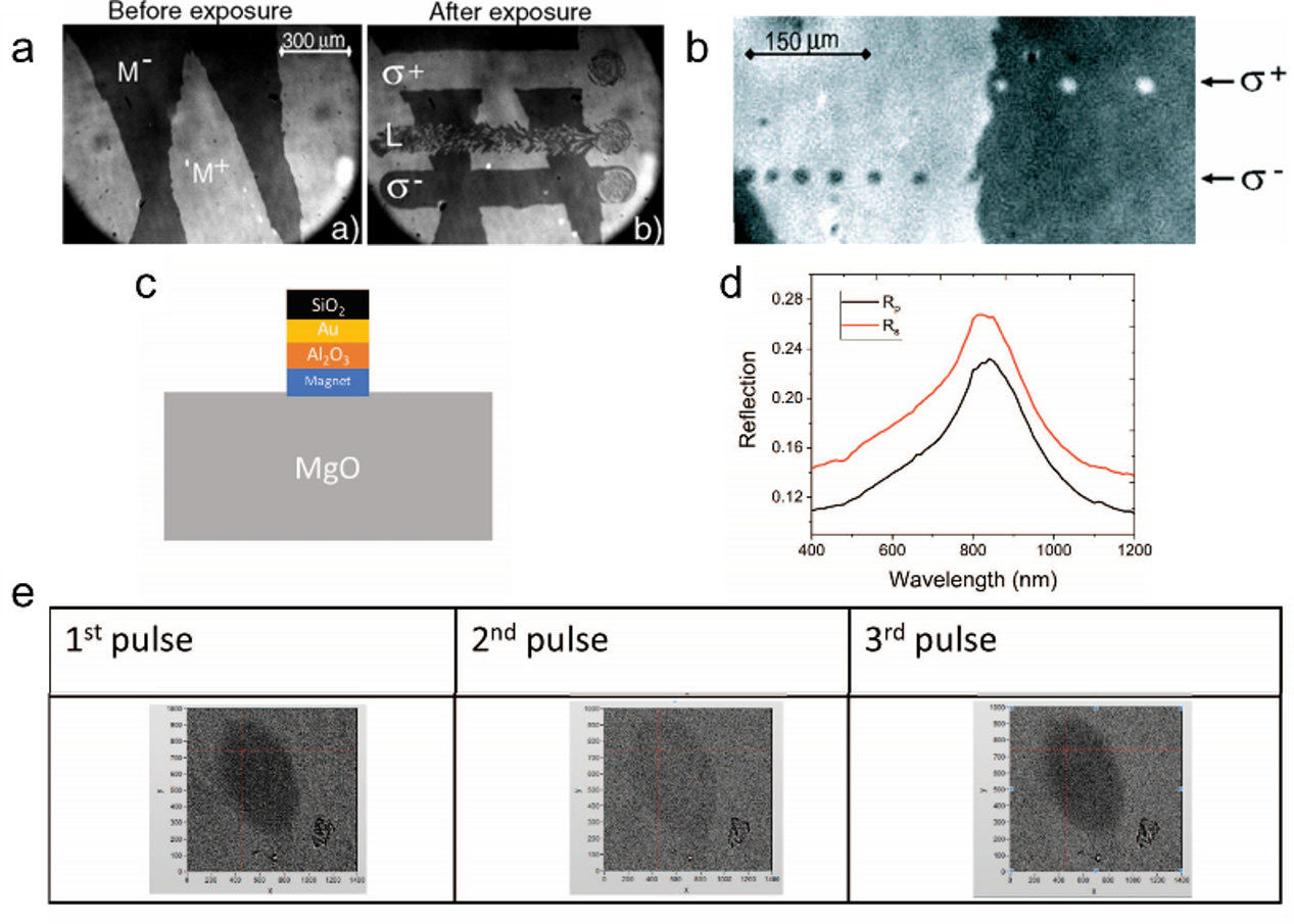
References:
[1] E. Beaurepaire, J.-C. Merle, A. Daunois, and J.-Y. Bigot, Phys. Rev. Lett. 76, 4250 (1996)
[2] A. Kirilyuk, A. V Kimel, and T. Rasing, Philos. Trans. A. Math. Phys. Eng. Sci. 369, 3631 (2011)
[3] C. D. Stanciu, F. Hansteen, A. V. Kimel, A. Kirilyuk, A. Tsukamoto, A. Itoh, and T. Rasing, Phys. Rev. Lett. 99, 1 (2007)
[4] I. Radu, K. Vahaplar, C. Stamm, T. Kachel, N. Pontius, H. A. Dürr, T. A. Ostler, J. Barker, R. F. L. Evans, R. W. Chantrell, A. Tsukamoto, A. Itoh, A. Kirilyuk, T. Rasing, and A. V Kimel, Nature 472, 205 (2011)
[5] J. H. Mentink, J. Hellsvik, D. V. Afanasiev, B. A. Ivanov, A. Kirilyuk, A. V. Kimel, O. Eriksson, M. I. Katsnelson, and T. Rasing, Phys. Rev. Lett. 108, 057202 (2012)
[6] A. Dutta, A. V. Kildishev, V. M. Shalaev, A. Boltasseva, and E. E. Marinero, Surface-plasmon opto-magnetic field enhancement for all-optical magnetization switching, Opt. Mater. Express 7(12), 4316-4327 (2017)
Epsilon-near-zero (ENZ) and Nonlinear Optics
Primary Contact: Soham Saha
Secondary Contacts: Zhaxylyk Kudyshev, Mustafa Ozlu
Collaborators: Prof. Daniele Faccio (Glasgow University), Marcello Ferrera, Heriot-Watt University
Advisors: Prof. Vladimir Shalaev, Prof. Alexandra Boltasseva
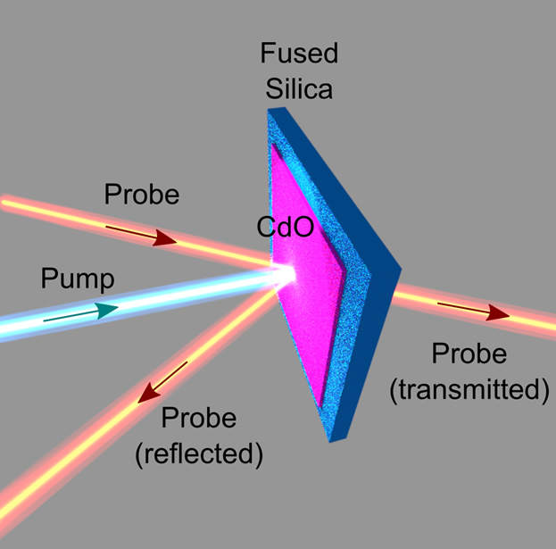
Many extraordinary optical phenomena are enhanced in the epsilon-near-zero (ENZ) regime - the wavelength regime where the complex permittivity of a material is near zero. The slow-light interactions in this regime increase light-matter interactions, bolstering phenomena such as enhanced nonlinearities [1], ultrafast reflection modulation [2], and emitter radiation engineering [3]. Transparent conducting oxides are natural homogeneous ENZ media and they exhibit extremely low-index behavior needed to realize the full potential of extraordinary nonlinear optics for photonics [4]. In this project, we investigate largely unexplored nonlinear optical phenomena in near-zero-index materials, enhanced by the extreme light-matter interaction resulting from the slow-light effect, without a need for complex nanostructure fabrication. Furthermore, the optical properties of these materials can be tuned by doping, thus enabling a great level of control over both the ENZ wavelength and the switching times [5]. We utilize low-loss transparent conducting oxides (TCOs) as homogeneous low index materials with the low-index region in the technologically relevant telecommunication spectrum [6]. We experimentally demonstrate nonlinear effects such as negative refraction [7] and broadband wavelength shifts [8] near the epsilon near zero region in aluminum-doped zinc oxide and tin-doped indium oxide. We also establish theories to better understand and predict the observed nonlinear enhancements. The findings of our research will enable the design of fast, low-loss, and efficient devices for optical modulation, beam steering, and optical isolator design.
References:
[1] Caspani, L.; Kaipurath, R. P. M.; Clerici, M.; Ferrera, M.; Roger, T.; Kim, J.; Kinsey, N.; Pietrzyk, M.; Di Falco, A.; Shalaev, V. M.; Boltasseva, A.; Faccio, D. Enhanced Nonlinear Refractive Index in ϵ -Near-Zero Materials. Phys. Rev. Lett. 2016, 116 (23), 233901. https://doi.org/10.1103/PhysRevLett.116.233901.
[2] Kinsey, N.; DeVault, C.; Kim, J.; Ferrera, M.; Shalaev, V. M.; Boltasseva, A. A. Epsilon-near-Zero Al-Doped ZnO for Ultrafast Switching at Telecom Wavelengths. Optica 2015, 2 (7), 616–622. https://doi.org/10.1364/OPTICA.2.000616.
[3] Kinsey, N.; DeVault, C.; Boltasseva, A.; Shalaev, V. M.; DeVault, C.; Boltasseva, A.; Shalaev, V. M. Near-Zero-Index Materials for Photonics. Nat. Rev. Mater. 2019, 4 (12), 1–19. https://doi.org/10.1038/s41578-019-0133-0.
[4] Kim, J.; Dutta, A.; Naik, G. V.; Giles, A. J.; Bezares, F. J.; Ellis, C. T.; Tischler, J. G.; Mahmoud, A. M.; Caglayan, H.; Glembocki, O. J.; Kildishev, A. V.; Caldwell, J. D.; Boltasseva, A.; Engheta, N. Role of Epsilon-near-Zero Substrates in the Optical Response of Plasmonic Antennas. Optica 2016, 3 (3), 339. https://doi.org/10.1364/OPTICA.3.000339.
[5] Saha, S.; Diroll, B. T.; Shank, J.; Kudyshev, Z.; Dutta, A.; Chowdhury, S. N.; Luk, T. S.; Campione, S.; Schaller, R. D.; Shalaev, V. M.; Boltasseva, A.; Wood, M. G. Broadband, High‐Speed, and Large‐Amplitude Dynamic Optical Switching with Yttrium‐Doped Cadmium Oxide. Adv. Funct. Mater. 2019, 1908377. https://doi.org/10.1002/adfm.201908377.
[6] Naik, G. V; Kim, J.; Boltasseva, A. Oxides and Nitrides as Alternative Plasmonic Materials in the Optical Range [Invited]. Opt. Mater. Express 2011, 1 (6), 1090. https://doi.org/10.1364/OME.1.001090.
[7] Vezzoli, S.; Bruno, V.; Devault, C.; Roger, T.; Shalaev, V. M.; Boltasseva, A.; Ferrera, M.; Clerici, M.; Dubietis, A.; Faccio, D. Optical Time Reversal from Time-Dependent Epsilon-Near-Zero Media. Phys. Rev. Lett. 2018, 120 (4), 043902. https://doi.org/10.1103/PhysRevLett.120.043902.
[8] Khurgin, J. B.; Clerici, M.; Bruno, V.; Caspani, L.; DeVault, C.; Kim, J.; Shaltout, A.; Boltasseva, A.; Shalaev, V. M.; Ferrera, M.; Faccio, D.; Kinsey, N. Adiabatic Frequency Shifting in Epsilon-near-Zero Materials: The Role of Group Velocity. Optica 2020, 7 (3), 226. https://doi.org/10.1364/OPTICA.374788.
[9] V. Bruno, C. DeVault, S. Vezzoli, Z. Kudyshev, T. Huq, S. Mignuzzi, A. Jacassi, S. Saha, Y. D. Shah, S. A. Maier, D. R. S. Cumming, A. Boltasseva, M. Ferrera, M. Clerici, D. Faccio, R. Sapienza, and V. M. Shalaev, Negative Refraction in Time-Varying Strongly Coupled Plasmonic-Antenna–Epsilon-Near-Zero Systems, Phys. Rev. Lett. v. 124, p. 043902 (2020)
[10] V. Bruno, S. Vezzoli, C. DeVault, T. Roger, M. Ferrera, A. Boltasseva, V.M. Shalaev, D. Faccio, Dynamical Control of Broadband Coherent Absorption in ENZ Films, Micromachines, v. 11, p. 110 (2020)
[11] V. Bruno, S. Vezzoli, C. DeVault, E. Carnemolla, M. Ferrera, A. Boltasseva, V. M. Shalaev, D. Faccio, M. Clerici, Broad Frequency Shift of Parametric Processes in Epsilon-Near-Zero Time-Varying Media, Applied Sciences, v. 10, p. 1318 (2020)
MURI: Near-Field Radiative Heat Transfer between Nanostructured Materials
Primary Contacts:
Zelong "Bruce" Ding,
Harsha Reddy,
Zhaxylyk Kudyshev
Advisors: Profs.
Vladimir Shalaev and
Alexandra Boltasseva
Collaborators: Profs. Pramod Reddy (UMich), Edgar Meyhofer (UMich), and Shanhui Fan (Stanford)
Short project description:
Illustration of NFRHT between two nanostructured metasurfaces separated by a nano gap
The principles of near-field (NF) radiative heat transfer (RHT), i.e. the transfer of heat or energy across nanoscale gaps via electromagnetic fields, are of great interest as several remarkable phenomena arise exclusively in the NF. Far-field (FF) RHT, explored at the beginning of the 20th century, culminated in Max Planck’s theory of RHT and played a central role in the development of quantum mechanics. However, Planck explicitly noted that his FFRHT theory was only applicable to scenarios where the separation between the hot and cold objects is significantly larger than the Wien’s wavelength (~10 μm at room temperature). With the advent of micro- and nanotechnology that features nanoscale dimensions, an urgent need to understand thermal radiation in nanoscale gaps has emerged.
Recent experiments have measured RHT rates in the NF [1-3], which have revealed several orders of magnitude enhancements in RHT rates, compared to FFRHT, when the separation between the hot and cold objects is reduced to length scales below Wein’s wavelength. Specifically, close to 1,000 fold enhancements in RHT were observed from experiments for gap sizes below 100 nm [3, 4]. These exciting discoveries have spurred researchers to explore ways to further engineer and enhance NFRHT. In this regard, recent theoretical studies [5-7] have predicted the possibility of further enhancing NFRHT via spectral engineering with metasurfaces that feature judiciously patterned nanostructures. Our group is currently working towards testing the validity of these interesting theoretical predictions. We are closely working with our collaborators (Prof. Shanhui Fan, Prof. Pramod Reddy and Prof. Edgar Meyhofer) towards fabricating these metasurfaces on suspended picowatt resolution calorimeters (designed and fabricated in Prof. Pramod Reddy and Prof. Edgar Meyhofer’s group). The performance of the fabricated metasurfaces will be characterized by our collaborators at University of Michigan, Ann Arbor, using their state-of-the-art nanopositioning platform. Along with their fundamental importance, these studies are expected to play a crucial role in the development of innovative thermal technologies, ranging from thermophotovoltaics to near-field photonic refrigeration.
References:
[1] Rousseau, E. et al. Radiative heat transfer at the nanoscale. Nat. Photonics. 3, 514-517 (2009).
[2] Shen, S. et al. Surface phonon polaritons mediated energy transfer between nanoscale gaps. Nano Lett. 9, 2909-2913 (2009).
[3] Kim, K. et al. Radiative heat transfer in the extreme near-field. Nature 528, 387-391 (2015).
[4] Song, B. et al. Radiative heat conductances between dielectric and metallic parallel plates with nanoscale gaps. Nat. Nanotechnol. 11, 509-514 (2016).
[5] Fernandez-Hurtado, V. et al. Enhancing Near-Field Radiative Heat Transfer with Si-Based Metasurfaces. Phys. Rev. Lett. 118, 203901 (2017).
[6] Miller, O.D. et al. Limits to the Optical Response of Graphene and Two-Dimensional Materials. Nano Letters 17, 5408-5415 (2017).
[7] Miller, O.D. et al. Shape-Independent Limits to Near-Field Radiative Heat Transfer. Phys. Rev. Lett. 115, 204302 (2015).
Mapping the nanoscale energy distributions of plasmonic hot-carriers
Contacts:
Harsha Reddy,
Zhaxylyk Kudyshev
Collaborators: Profs.
Pramod Reddy and
Edgar Meyhofer (University of Michigan, Ann Arbor)
Advisors: Profs. Vladimir Shalaev, Alexandra Boltasseva, and Alexander Kildishev
The generation of hot-carriers in plasmonic nanostructures, via plasmon decay, is of great current interest as hot-carriers play key roles in applications like photocatalysis, energy harvesting and in novel photodetection schemes that circumvent band-gap limitations. However, experimental quantification of steady-state energy distributions of hot-carriers in plasmonic nanostructures, which is critical for systematic progress, has not been possible. To address this outstanding challenge, we recently developed an experimental approach that enabled the direct measurement of hot-carrier energy distributions under steady-state conditions [1]. Specifically, we combined scanning probe-based quantum transport measurement techniques that record charge transport through single molecular junctions with nanoplasmonic experimental methods to directly quantify hot-carrier energy distributions in a key model system—a thin gold film that supports propagating surface plasmon polaritons. Furthermore, from our measurements, we obtained key physical insights on the role of Landau damping in producing hot-carriers and the contributions of different plasmonic modes towards hot-carrier generation. These studies were done in collaboration with Prof. Pramod Reddy and Prof. Edgar Meyhofer’s group at the University of Michigan, Ann Arbor.
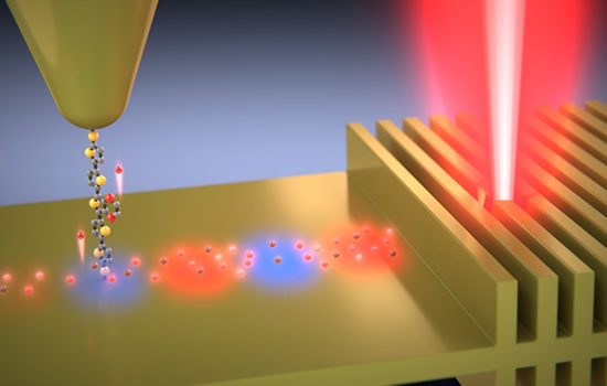
On the left, graphic representation of the experimental approach to determine the energy distributions of plasmonic hot-carriers in a thin gold film. Surface plasmon polaritons are excited by illuminating the grating coupler with a laser, which leads to the generation of hot-carriers. The energy distributions of the generated hot-carriers are measured from the current flowing through a (voltage controlled) tunable molecular filter that selectively allows transport of carriers in a narrow energy window.
References:
[1] H. Reddy, K. Wang, Z. Kudyshev, L. Zhu, S. Yan, A. Vezzoli, S. J. Higgins, V. Gavini, A. Boltasseva, P. Reddy, V. M. Shalaev, and E. Meyhofer, "Determining plasmonic hot-carrier energy distributions via single molecule transport measurements,” Science, 10.1126/science.abb3457, 2020.
Quantum Nano-optics
Primary Contacts: Dr. Demid Sychev, Dr. Alexander Senichev
Secondary Contacts: Dr. Zhaxylyk Kudyshev, Xiaohui Xu, Zach Martin, Dr. Alexei Lagoutchev (Purdue)
Collaborators: Prof. Simeon Bogdanov, Prof. Alexey V. Akimov, Prof. Igor Aharonovitch, Prof. Jacob Khurgin, Prof. Sergey I. Bozhevolnyi, Prof. Ilya A. Rodionov
Advisors: Profs. Vladimir Shalaev, Alexandra Boltasseva, and Alexander Kildishev
Short project description:
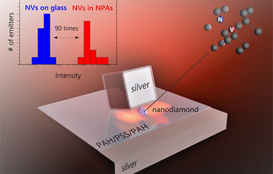
Color centers in diamond are crystalline defects that share many quantum properties with single atoms. At the same time, they are easier to manipulate than the latter and can be integrated into various solid-state devices. They are also promising platforms for realizing quantum devices such as nanoscale sensors, single-photon sources or quantum memories. Our research aims at discovering whether it is possible to draw on the potential of the dynamic field of nanophotonics in order to enhance or better harness the quantum properties of such systems. In particular, novel nanophotonic structures such as hyperbolic metamaterials, plasmonic waveguides, and plasmonic nanocavities are good candidates for increasing color centers’ spontaneous emission rate and controlling the directionality of their emission over a broad frequency range. The use of CMOS-compatible epitaxially grown plasmonic materials in the design of plasmonic structures promises a new level of functionality for a variety of integrated room-temperature quantum devices based on diamond color centers.
In the scope of this project, we have examined different types of nanodiamonds and identified the characteristics that lead to optimal optical and chemical properties. We have demonstrated broadband enhancement of emission from nitrogen-vacancy (NV) centers in nanodiamonds for both single NV centers and ensembles of NV centers using hyperbolic metamaterials (HMM), nanopatch antennas (NPA), and integrated plasmonic launchers (PL). As part of this work, we have studied the correlations between Purcell factor and optical measurements of NV’s spin state and the possibility to perform nanoscale sensing of photonic density of states using NV’s spin properties. By reducing the fluorescence lifetime from single NV centers, we also hope to enhance their single-photon emission rate such that we can perform a single-shot measurement of an NV center’s spin state. At the same time, we are also interested in developing nanoscale quantum devices from silicon-vacancy (SiV), germanium-vacancy (GeV), and lead-vacancy (PbV) centers in nanodiamonds. By enhancing the rate of emission from these defects, it may be possible to produce indistinguishable photons at room temperature. Similarly, we are also interested in developing quantum emitters in new materials such as 2D perovskite nanocrystals, transition metal dichalcogenide (TMDC) bilayers, and hexagonal boron nitride (hBN) flakes. Finally, we collaborate with other research groups to use defect centers in nanodiamonds and other materials for quantum sensing applications.
Papers Published:
- M. Y. Shalaginov, G. V. Naik, S. Ishii, M. N. Slipchenko, A. Boltasseva, J.-X. Cheng, A. N. Smolyaninov, E. Kochman, and V. M. Shalaev. "Characterization of nanodiamonds for metamaterial applications," Appl.Phys.B 105, 2, 191-195 (2011)
- M. Y. Shalaginov, S Ishii, J Liu, A Kildishev, VM Shalaev, "Broadband enhancement of spontaneous emission from nitrogen-vacancy centers in nanodiamonds by hyperbolic metamaterials" in 2013 Conference on Lasers and Electro-Optics (CLEO) and Quantum Electronics and Laser Science Conference (QELS), San Jose, CA, USA, 2013
- M. Y. Shalaginov, S.Ishii, J. Liu, J. Liu, J. Irudayaraj, A. Lagutchev, A.V. Kildishev, and V. M. Shalaev, "Broadband enhancement of spontaneous emission from nitrogen-vacancy centers in nanodiamonds by hyperbolic metamaterials", Appl. Phys. Lett. 102, 173114 (2013)
- M. Y. Shalaginov, V. V. Vorobyov, J. Liu, Marcello Ferrera, A. V. Akimov, A. Lagutchev, A. N. Smolyaninov, V. V. Klimov, J. Irudayaraj, A. V. Kildishev, A. Boltasseva and V. M. Shalaev, "Single-photon source based on NV center in nanodiamond coupled to TiN-based hyperbolic metamaterial" in 2014 Conference on Lasers and Electro-Optics (CLEO) and Quantum Electronics and Laser Science Conference (QELS), San Jose, CA, USA, 2014
- M. Y. Shalaginov, V. V. Vorobyov, J. Liu, M. Ferrera, A. V. Akimov, A. Lagutchev, A. N. Smolyaninov, V. V. Klimov, J. Irudayaraj, A. V. Kildishev, A. Boltasseva, and V. M. Shalaev, "Enhancement of single-photon emission from nitrogen-vacancy centers with TiN/(Al,Sc)N hyperbolic metamaterials", Laser Photonics Rev., 9, 1, 120-127 (2015) (*Cover Article*)
- M. Y. Shalaginov, A. Lagutchev, V. M. Shalaev, and A. V. Kildishev, "Effect of a hyperbolic metamaterial on radiation patterns of a single-photon source", in 2015 Conference on Lasers and Electro-Optics (CLEO) and Quantum Electronics and Laser Science Conference (QELS), San Jose, CA, USA, 2015
- S. Bogdanov, M. Y. Shalaginov, A. Akimov, P. Kapitanova, J. Liu, D. Woods, M. Ferrera, A. S. Laguchev, P Belov, J. Irudayaraj, A. Boltasseva, and V. M. Shalaev, "Engineering the spin-flip induced fluorescence contrast of diamond nitrogen
- O. A. Makarova, M. Y. Shalaginov, S. Bogdanov, A. V. Kildishev, A. Boltasseva, and V. M. Shalaev, Patterned multilayer metamaterial for fast and efficient photon collection from dipolar emitters, Optics Letters, Vol. 42, Issue 19, pp. 3968-3971 (2017)
- S. Bogdanov, M. Y. Shalaginov, A. Boltasseva, and V. M. Shalaev, Material platforms for integrated quantum photonics, Opt. Mater. Express 7, 111-132 (2017)
- S. Bogdanov, M. Y. Shalaginov, A. Akimov, A. S. Lagutchev, P. Kapitanova, J. Liu, D. Woods, M. Ferrera, P. Belov, J. Irudayaraj, A. Boltasseva, and V. M. Shalaev, Electron spin contrast of Purcell-enhanced nitrogen-vacancy ensembles in nanodiamonds, Phys. Rev. B 96, 035146 (2017)
- Simeon I. Bogdanov, Mikhail Y. Shalaginov, Alexei S. Lagutchev, Chin-Cheng Chiang, Deesha Shah, Alexandr S. Baburin, Ilya A. Ryzhikov, Ilya A. Rodionov, Alexander V. Kildishev, Alexandra Boltasseva, and Vladimir M. Shalaev, Ultrabright Room-Temperature Sub-Nanosecond Emission from Single Nitrogen-Vacancy Centers Coupled to Nanopatch Antennas, Nano Letters (2018)
- S.I. Bogdanov, A. Boltasseva, and V.M. Shalaev, Overcoming quantum decoherence with plasmonics, Science, v. 364, pp. 532-533 (2019)
- S. I. Bogdanov, O. A. Makarova, X. Xu, Z. O. Martin, A. S. Lagutchev, M. Olinde, D. Shah, S. N. Chowdhury, A. R. Gabidullin, I. A. Ryzhikov, I. A. Rodionov, A. V. Kildishev, S. I. Bozhevolnyi, A. Boltasseva, V. M. Shalaev, and J. B. Khurgin, Ultrafast quantum photonics enabled by coupling plasmonic nanocavities to strongly radiative antennas, Optica v. 7, pp. 463-469 (2020)
Robust Vivid Plasmonic Color Printing
Primary Contact: Sarah Nahar Chowdhury
SAdditional Contacts: Dr. Alexei S. Lagoutchev, Zhaxylyk Kudyshev
Collaborators: Dr. Piotr Nyga, Dr. Esteban Garcia
Advisors: Profs. Vladimir Shalaev, Alexandra Boltasseva, Alexander Kildishev
Short project description:
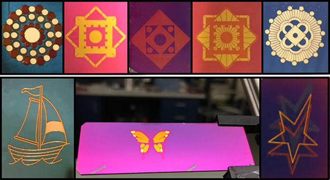
We demonstrate a method of generation of bright colors through laser post processing on a multilayer structure comprising of a very thin layer of Ag semicontinuous metal film (SMF) on a dielectric spacer with mirror. Such a structure is not only inexpensive, environment-friendly, and non-bleaching but also has the potential of microscopic printing to 1.44µm (approx.). The process employs a SMF comprising of random nanostructures with different particle sizes and shapes which are responsible for absorption at different wavelengths. SMF on spacer with mirror (SMFM) upon interaction with light can localize electromagnetic energy in nanoscale regions. With laser illumination, reshaping and fragmentation of metallic nanostructures occur in the vicinity of these regions and change in optical response occurs. Through varying the scan speed, number of pulses, energy density, power, and exposure time of 800 nm, 80 fs, 1 kHz laser illuminated on the structure, highly contrasting and vivid colors can be obtained. This structure can be fabricated easily and can be applied to the macroscopic, mesoscopic and nanoscopic printing of innovatory fade-free artistic images as one example of application.
Papers Published:
[1] Laser-induced color printing on semicontinuous silver films: red, green and blue, Piotr Nyga, Sarah N Chowdhury, Zhaxylyk Kudyshev, Mark D Thoreson, Alexander V Kildishev, Vladimir M Shalaev, Alexandra Boltasseva, Optical Materials Express 9 (3), 1528-1538
[2] Laser Color Printing on Semicontinuous Silver Films, Sarah N Chowdhury, Piotr Nyga, Zhaxylyk Kudyshev, Alexander V Kildishev, Vladimir M Shalaev, Alexandra Boltasseva, CLEO: Science and Innovations, JW2A. 55
[3] Laser Color Printing on Semicontinuous Ag Films, Sarah N. Chowdhury, Piotr Nyga, Zhaxylyk Kudyshev, Alexander V. Kildishev, Vladimir M. Shalaev, Alexandra Boltasseva, Women in Engineering Program 50th Anniversary Celebration
Transdimensional Plasmonic Materials
Primary Contact: Deesha Shah
Collaborators: Prof. Igor Bondarev (North Carolina Central University), Dr. Arrigo Calzolari (CNR-Nano, Italy)
Advisors: Profs. Vladimir Shalaev and Alexandra Boltasseva
Short project description:
![]()
As plasmonic materials transition from the three dimensional (3D) form to two dimensional (2D), unique optical and electronic phenomena arise that are unattainable in bulk materials and conventional thin films. Similar to 2D materials, ultra-thin films in the transdimensional regime spanning a few atomic layers, known as transdimensional materials (TDMs), are expected to exhibit strong dependences on structural and compositional properties, as well as extreme sensitivities to external optical and electrical perturbations. Additionally, the small thicknesses may lead to strongly confined surface plasmons and unique quantum phenomena such as forbidden atomic transitions and enhanced nonlinearities. The strong tunability and light confinement offered by TDMs has resulted in a search for atomically thin material platforms that facilitate active metasurfaces with novel functionalities in the visible and NIR range.
Epitaxial thin films are particularly ideal in investigating the size dependent response as there are no contributions to losses from grain boundaries. Epitaxial TiN can be routinely grown on substrates such as c-sapphire and MgO with standard sputtering processes, enabling the formation of continuous ultrathin films down to 1 nm (5 monolayers) while maintaining high quality. Due to its high-quality growth, chemical stability, and tailorable optical properties, TiN is an ideal material choice to study plasmonic properties at the atomic level. We are investigating the thickness dependent properties of ultra-thin TiN experimentally and theoretically, which hold great promise for realizing a new generation of tunable metasurfaces with quantum and nonlocal effects.
Papers:
[1] Shah, D., Kudyshev, Z. A., Saha, S., Shalaev, V. M. & Boltasseva, A. Transdimensional material platforms for tunable metasurface design. MRS Bull. 45, 188–195 (2020).
[2] Boltasseva, A. & Shalaev, V. M. Transdimensional Photonics. ACS Photonics 6, 1–3 (2019).
[3] Shah, D. et al. Controlling the Plasmonic Properties of Ultrathin TiN Films at the Atomic Level. ACS Photonics 5, 2816–2824 (2018).
[4] Bondarev, I. V., Mousavi, H. & Shalaev, V. M. Optical response of finite-thickness ultrathin plasmonic films. MRS Commun. 8, 1092–1097 (2018).
[5] Bondarev, I. V. & Shalaev, V. M. Universal features of the optical properties of ultrathin plasmonic films. Opt. Mater. Express 7, 3731–3740 (2017).
[6] Shah, D., Reddy, H., Kinsey, N., Shalaev, V. M. & Boltasseva, A. Optical Properties of Plasmonic Ultrathin TiN Films. Adv. Opt. Mater. 5, 1700065 (2017).
Refractory Plasmonics
Team members: Bruce Ding, Sam Peana, Harsha Reddy, Karthik Pagadala
Advisors: Prof. Vladimir M. Shalaev, Prof. Alexandra Boltasseva, Prof. Alexander Kildishev
Collaborators: Prof. Ernesto Marinero, Prof. Peter Bermel, Prof. Tim Sands, Prof. Ali Shakouri, Prof. Ted Norris, Prof. Oana Malis, Prof. Sergey Bozhevolnyi
Short project description:
Some of the proposed plasmonic applications require extreme operating conditions such as high temperatures and chemically aggressive environment. Conventional plasmonic materials such as noble metals bring limitations due to their lower melting point, softness etc. Refractory materials, exhibiting high melting points and chemical stability above 2000 oC, with plasmonic properties in the visible and near infrared regions can be the solutions to major problems hindering the improvement of potentially high-impact applications such as heat assisted magnetic recording (HAMR), solar/thermophotovoltaics (S/TPV) and solar thermoelectric generators (STEG).
Transition metal nitrides, in particular titanium nitride (TiN) and zirconium nitride (ZrN), are known as refractory materials and exhibit plasmonic resonances in the visible and near infrared regions. Nanoantennas made of refractory plasmonic materials can be employed as durable near field transducers for HAMR heads where antenna temperatures are estimated to be above 400°C. Furthermore, ultrathin broadband absorbers and selective emitters made of refractory plasmonic materials offer durability at higher temperatures and higher overall device efficiencies for S/TPVs and STEGs.
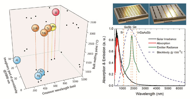
Papers:
- J. Liu, U. Guler, A. Lagoutchev, A. Kildishev, O. Malis, A. Boltasseva, V. M. Shalaev, "Quasi-coherent thermal emitter based on refractory plasmonic materials", Opt. Mater. Express, v. 5, pp. 2721-2728 (2015)
- U. Guler, S. Suslov, A. V. Kildishev, A. Boltasseva, V. M. Shalaev, "Colloidal plasmonic titanium nitride nanoparticles: Properties and applications", Nanophotonics, DOI: 10.1515/nanoph-2015-0017 (*Invited Research Paper*)
- U. Guler, A. Boltasseva, V. M. Shalaev, "Plasmonics on the slope of enlightenment: the role of transition metal nitrides", Faraday Discuss. 178, 71-86 (2015) (*Invited Research Paper*)
- U. Guler, V. M. Shalaev, and A. Boltasseva, "Nanoparticle Plasmonics: Going Practical with Transition Metal Nitrides," Materials Today, 18, 227-237 (2015) (*Invited Review Paper*)
- W. Li, U. Guler, N. Kinsey, G. V. Naik, A. Boltasseva, J. Guan, V. M. Shalaev, and A. V. Kildishev, "Refractory Plasmonics with Titanium Nitride: Broadband Metamaterial Absorber," Adv. Mater. 26, 7959-7965 (2014). (*Cover Article*)
- U. Guler, A. Boltasseva, and V. M. Shalaev, Refractory Plasmonics, Science 344, 263-264 (2014)
- U. Guler, J. C. Ndukaife, G. V. Naik, A. G. A. Nnanna, A. V. Kildishev, V. M. Shalaev, and A. Boltasseva, Local Heating with Lithographically Fabricated Plasmonic Titanium Nitride Nanoparticles, Nano Letters 13, 6078-6083 (2013)
- U. Guler, G. V. Naik, A. Boltasseva, V. M. Shalaev, and A. V. Kildishev, Performance Analysis of Nitride Alternative Plasmonic Materials for Localized Surface Plasmon Applications, Appl. Phys. B 107, 285-291 (2012)
- Urcan Guler, Wei Li, Alexandra Boltasseva, Alexander Kildishev, Vladimir M. Shalaev, "Titanium Nitride as a Refractory Plasmonic Material for High Temperature Applications," in CLEO: 2014
- Jingjing Liu, Urcan Guler, Wei Li, Alexander V. Kildishev, Alexandra Boltasseva, and Vladimir M. Shalaev, "High-temperature plasmonic thermal emitter for thermo-photovoltaics," in CLEO: 2014
- U. Guler, W. Li, N. Kinsey, G. V. Naik, A. Boltasseva, J. Guan, A. V. Kildishev, and V. M. Shalaev, Plasmonic Titanium Nitride Nanostructures for Perfect Absorbers, in Renewable Energy and the Environment, OSA Technical Digest (online) (Optical Society of America, 2013), PW3B.8
- U. Guler, G. Naik, A. Boltasseva, V. Shalaev, and A. Kildishev, Nitrides as alternative materials for localized surface plasmon applications, in Frontiers in Optics 2012/Laser Science XXVIII, OSA Technical Digest (online) (Optical Society of America, 2012), FTh4A.2
- K. Chaudhuri, U. Guler, S. Azzam, H. Reddy, S. Saha, E. Marinero, A. V. Kildishev, V. M Shalaev, A. Boltasseva, Remote Sensing of High Temperatures with Refractory, Direct-Contact Optical Metacavity, ACS Photonics (2020)
- K. Chaudhuri, U. Guler, S. Azzam, H. Reddy, S. Saha, E. Marinero, A. V. Kildishev, V. M. Shalaev, A. Boltasseva, Remote Sensing of High Temperatures with Refractory, Direct-Contact Optical Metacavity, ACS Photonics, v. 7, pp. 472–479 (2020)
Quantum Nanophotonics with Color Centers in Diamond
Primary Contact: Dr. Demid Sychev
Advisors: Prof. Alexander Kildishev, Prof. Vladimir Shalaev
Additional Contact: Dr. Alexei S. Lagoutchev
Collaborators: Dr. Alexey V. Akimov (RQC), Dr. Mikhail Y. Shalaginov, Prof. Simeon Bogdanov
Short project description:
Color centers in diamond are crystalline defects that share many quantum properties with single atoms. At the same time they are easier to manipulate than the latter and can be integrated into a solid state infrastructure. They are promising for realizing quantum devices such as nanoscale sensors, single-photon sources or quantum memories. Our research aims at discovering whether it is possible to draw on the promising potential of the fast developing field of nanophotonics in order to enhance or better harness the quantum properties of such systems. In particular, novel nanophotonic structures such as hyperbolic metamaterials and plasmonic waveguides are good candidates for increasing the color center's spontaneous emission rate and controlling the directionality of their emission in a broad frequency range. The broadband optical Purcell factor in plasmonic systems can be also used to control the spin readout. Conversely, the color centers' spin degree of freedom can simplify the measurement of the photonic density of states on the nanoscale. The use of CMOS-compatible epitaxially grown plasmonic materials in the design of plasmonic structures promises a new level of functionality for a variety of integrated room-temperature quantum devices based on diamond color centers.
In the scope of this project, we have examined different types of nanodiamonds and identified the characteristics that lead to optimal optical and chemical properties. We have demonstrated broadband enhancement of emission from nitrogen-vacancy (NV) center ensembles in nanodiamonds using conventional gold/alumina hyperbolic metamaterials (HMM). We have theoretically shown that planar multilayer HMM make single photon emission more directional. We have showed both the fluorescence lifetime reduction and the enhancement of single-photon emission from single NV centers in nanodiamonds coupled to an epitaxially grown CMOS-compatible HMM made of novel plasmonic materials TiN/AlScN. In our most recent work, we have studied the correlations between Purcell factor and optical measurements of NV’s spin state and the possibility to perform nanoscale sensing of photonic density of states using NV’s spin properties. Our results may enable CMOS-compatible integrated quantum devices operating at room temperature.
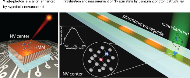
Papers Published:
- M. Y. Shalaginov, G. V. Naik, S. Ishii, M. N. Slipchenko, A. Boltasseva, J.-X. Cheng, A. N. Smolyaninov, E. Kochman, and V. M. Shalaev. "Characterization of nanodiamonds for metamaterial applications," Appl.Phys.B 105, 2, 191-195 (2011)
- M. Y. Shalaginov, S Ishii, J Liu, A Kildishev, VM Shalaev, Broadband enhancement of spontaneous emission from nitrogen-vacancy centers in nanodiamonds by hyperbolic metamaterials in 2013 Conference on Lasers and Electro-Optics (CLEO) and Quantum Electronics and Laser Science Conference (QELS), San Jose, CA, USA, 2013
- M. Y. Shalaginov, S.Ishii, J. Liu, J. Liu, J. Irudayaraj, A. Lagutchev, A.V. Kildishev, and V. M. Shalaev, "Broadband enhancement of spontaneous emission from nitrogen-vacancy centers in nanodiamonds by hyperbolic metamaterials", Appl. Phys. Lett. 102, 173114 (2013)
- M. Y. Shalaginov, V. V. Vorobyov, J. Liu, Marcello Ferrera, A. V. Akimov, A. Lagutchev, A. N. Smolyaninov, V. V. Klimov, J. Irudayaraj, A. V. Kildishev, A. Boltasseva and V. M. Shalaev, "Single-photon source based on NV center in nanodiamond coupled to TiN-based hyperbolic metamaterial" in 2014 Conference on Lasers and Electro-Optics (CLEO) and Quantum Electronics and Laser Science Conference (QELS), San Jose, CA, USA, 2014
- M. Y. Shalaginov, V. V. Vorobyov, J. Liu, M. Ferrera, A. V. Akimov, A. Lagutchev, A. N. Smolyaninov, V. V. Klimov, J. Irudayaraj, A. V. Kildishev, A. Boltasseva, and V. M. Shalaev, "Enhancement of single-photon emission from nitrogen-vacancy centers with TiN/(Al,Sc)N hyperbolic metamaterials", Laser Photonics Rev., 9, 1, 120-127 (2015) (*Cover Article*)
- M. Y. Shalaginov, A. Lagutchev, V. M. Shalaev, and A. V. Kildishev, "Effect of a hyperbolic metamaterial on radiation patterns of a single-photon source", in 2015 Conference on Lasers and Electro-Optics (CLEO) and Quantum Electronics and Laser Science Conference (QELS), San Jose, CA, USA, 2015
- S. Bogdanov, M. Y. Shalaginov, A. Akimov, P. Kapitanova, J. Liu, D. Woods, M. Ferrera, A. S. Laguchev, P Belov, J. Irudayaraj, A. Boltasseva, and V. M. Shalaev, "Engineering the spin-flip induced fluorescence contrast of diamond nitrogen
- M. Y. Shalaginov, S. Bogdanov, A. S. Lagutchev, A. V. Kildishev, A. Boltasseva, and V. M. Shalaev, On-chip Single-layer Integration of Diamond Spins with Microwave and Plasmonic Channels, ACS Photonics 2020, Publication Date: July 20, 2020; https://doi.org/10.1021/acsphotonics.0c00325
Cloud Computing Nanophotonics Tools @ nanoHUB.org
Primary Contact: Dr. Zhaxylyk Kudyshev
Additional Contact: Dr. Ludmila Prokopeva
Advisors: Prof. Alexander Kildishev, Prof. Vladimir Shalaev
Collaborators: Dr. Xingjie Ni, Dr. Satoshi Ishii, Dr. Zhengtong Liu, Dr. Uday. K. Chettiar, Jan Trieschmann
Short project description:
We developed simulation tools for nanophotonics, staged at www.nanoHUB.org to deliver a scientific application as a cloud computing service. Our on-line tools provide electromagnetic and multiphysics simulations of planar, circular and spherical multilayered nanophotonic devices, the full list is:
- PhotonicsDB: approximating and comparing the frequency dispersive optical properties of various materials
- PhotonicsRT: designing planar nanostructured lamellar photonic crystals and non-reflecting coatings
- PhotonicsSHA-2D: user customized cascaded photonic or plasmonic 2D metamaterials
- PhotonicsCL: user-customized cylindrical transformation optics lenses
- PhotonicsGAIN-0D: simulations of active media described by a four-level atomic system
- PhotonicsPOS: scattering solutions for a multi-shell spherical particle on a planar multi-layered substrate
- PhotonicVASEfit: Retrieves optical constants of a material by fitting it to VASE (Variable Angle Spectroscopic Ellipsometry) data


Publications and other contributions:
- Ludmila Prokopeva; You-Chia Chang; Alexander V. Kildishev (2015), "PhotonicVASEfit: VASE fitting tool," https://nanohub.org/resources/photonicvasefit. (DOI: 10.4231/D3JH3D373)
- Rohith Chandrasekar; Urcan Guler; Ludmila Prokopeva; Alexander V. Kildishev (2015), "PhotonicsPOS: Particle on Substrate," https://nanohub.org/resources/photonicspos. (DOI: 10.4231/D3S756M23)
- J. Fang, J. Liu, Z. Wang, X. Meng, L. Prokopeva, V. M. Shalaev, and A. V. Kildishev, "Time-Domain Model of 4-Level Gain System Fitted to Nanohole Array Lasing Experiment," in CLEO: 2015, OSA Technical Digest (online) (Optical Society of America, 2015), paper FW3E.5
- J. Fang; L. Prokopeva; J. Trieschmann; N. Arnold; A. V. Kildishev (2013), "PhotonicsGAIN-0D," http://nanohub.org/resources/testgain0d. (DOI: 10.4231/D3PK07200)
- Satoshi Ishii; Uday K. Chettiar; Xingjie Ni; Alexander V. Kildishev (2012), "PhotonicsRT: Wave Propagation in Multilayer Structures," https://nanohub.org/resources/photonicsrt. (DOI: 10.4231/D3BG2H902)
- Xingjie Ni; Zhengtong Liu; Fan Gu; Marcos Gabriel Pacheco; Joshua Borneman; Alexander V. Kildishev (2012), "PhotonicsSHA-2D: Modeling of Single-Period Multilayer Optical Gratings and Metamaterials," https://nanohub.org/resources/sha2d. (DOI: 10.4231/D3WS8HK4X)
- J. Trieschmann, S. Xiao, L. J. Prokopeva, V. P. Drachev, and A. V. Kildishev, "Experimental retrieval of the kinetic parameters of a dye in a solid film" Optics Express, Vol. 19, Issue 19, 18253-18259 (2011)
- Xingjie Ni; Fan Gu; Ludmila Prokopeva; Alexander V. Kildishev (2011), "PhotonicsCL: Photonic Cylindrical Multilayer Lenses," https://nanohub.org/resources/photonicscl. (DOI: 10.4231/D3Q52FC6B)
- Xingjie Ni; Zhengtong Liu; Alexander V. Kildishev (2010), "PhotonicsDB: Optical Constants," https://nanohub.org/resources/PhotonicsDB. (DOI: 10.4231/D3FT8DJ4J)
Novel Optics with Metasurfaces
Primary Contact: Soham Saha
Additional Contact: Deesha Shah, Sarah Nahar Chowdhury
Advisors: Prof. Vladimir Shalaev, Prof. Alexandra Boltasseva, Prof. Alexander Kildishev
Collaborator: Dr. Amr Shaltout
Short project description:

Subwavelength cavities are obtained by replacing conventional mirrors with reflecting metasurfaces that introduce arbitrary phase-shifts compensating for reduced accumulated phase through the ultra-small cavity. Same concept works for waveguides, where propagating modes require round trip phase-shift in the transverse direction to be integer multiple of 2p. This causes the minimum cross-section size to be the diffraction limit of ?/2, and introducing reflecting metasurfaces change the phase condition allowing the cross-section to go below the diffraction limit.

We design, fabricate, and experimentally demonstrate optically active metasurfaces of ?/50 thickness. Our approach is built on supercell metasurface design methodology: by judiciously designing the location and orientation of individual antennas in the structural supercells, we achieve effective chiral metasurfaces through a collective operation of non-chiral antennas.

Ultrathin metamaterial layers are modeled by a homogeneous bi-anisotropic film to model various kinds of broken symmetries in photonic nanostructures. It successfully modeled rotational asymmetry, mirror asymmetry and directional asymmetry. It has been also used to replace an array of nanostructured plasmonic elements (e.g. V-shape antennas) with a thin metasurface of equivalent bianisotropic tiles, which enabled significant reduction of computational load for simulation purposes.
Papers Published:
- A. M. Shaltout, A. V. Kildishev, and V. M. Shalaev "Ultra-Small Cavity with Reflecting Metasurfaces", US patent application
- A. M. Shaltout, A. V. Kildishev, V. M. Shalaev, "Compact Subwavelength Cavities Using Reflecting Metasurfaces," Accepted for 2014 Conference on Lasers and Electro-Optics (CLEO) and Quantum Electronics and Laser Science Conference (QELS), San Jose, CA, USA, 2014
- A. M. Shaltout, V. M. Shalaev, and A. V. Kildishev "Waveguides with Hyperbolic Metasurface Claddings", ACES 2014 Conference, Jacksonsville, Fl, USA, 2014. (4th place winner of student paper competition)
- P.R. West, J. L. Stewart, A. Kildishev, V.M. Shalaev, V. Shkunov, F. Strohkendl, Y. Zakharenkov, R. Dodds, R. Byren, "All-dielectric subwavelength metasurface focusing lens," submitted to Optics Express, 2014
- A. M. Shaltout, J. Liu, V. M. Shalaev, and A. V. Kildishev, "Optically Active Metasurfaces with Nonchiral Plasmonic Nano-antennas" submitted for journal publication
- A. M. Shaltout, J. Liu, A. V. Kildishev, and V. M. Shalaev, Broadband Optical Chirality Using Ultrathin Metasurface, in 2013 Conference on Lasers and Electro-Optics (CLEO) and Quantum Electronics and Laser Science Conference (QELS), San Jose, CA, USA, 2013
- F. Ding, N. Kinsey, J. J. Liu, Z. X. Wang; V. M. Shalaev and A. V. Kildishev, "Unidirectional Surface Plasmon Polariton Coupler in the Visible Using Metasurfaces," Accepted for 2014 Conference on Lasers and Electro-Optics (CLEO) and Quantum Electronics and Laser Science Conference (QELS), San Jose, CA, USA, 2014
- J. Liu, A. M. Shaltout, X. Ni, V. M. Shalaev, and A. V. Kildishev, "Approximating metasurfaces with bianisotropic tiles" ACES 2014 Conference (Invited paper), Jacksonsville, Fl, USA, 2014
- J. Liu, A. M. Shaltout, X. Ni, V. M. Shalaev, A. V. Kildishev, Experimental validation of a new bianisotropic parameter retrieval technique using plasmonic metasurfaces made of V-shape antennas, in The SPIE Optics+Photonics 2013 Advance, San Diego, CA, USA, 2013
- A. M. Shaltout, V. M. Shalaev, A. V. Kildishev, Homogenization of bi-anisotropic metasurfaces, Optics Express, Vol 21, Issue 19, pp. 21941 - 21950 (2013)
- A. M. Shaltout, V. M. Shalaev, A. V. Kildishev, "Bi-Anisotropic Homogenization of Metasurfaces," ACES 2013 Conference, Monterey, CA, USA, 2013
- A.M. Shaltout, V.M. Shalaev, M.L. Brongersma, Spatiotemporal light control with active metasurfaces, Science 364, eaat3100 (2019). DOI: 10.1126/science.aat3100
- A. M. Shaltout , K. G. Lagoudakis, J. van de Groep, S. J. Kim, J. Vučković, V. M. Shalaev, M. L. Brongersma, Spatiotemporal light control with frequency-gradient metasurfaces, Science, v. 365, pp. 374-377 (2019); DOI: 10.1126/science.aax2357
Nanolasers
Primary Contact: Dr. Xiangeng Meng
Additional Contact: Dr. Alexei S. Lagoutchev
Advisors: Prof. Vladimir Shalaev, Prof. Alexandra Boltasseva, Prof. Alexander Kildishev
Short project description:
The nanolaser project aims to develop compact light sources using plasmonic nanostructures as resonant cavities. The nanolaser is based on amplification of surface plasmons ? surface waves propagating along a metallic-dielectric interface, thus also entitled spaser (short for surface plasmon amplification by stimulated emission of radiation). The fact that plasmon modes have no cutoff allows for creation of compact light sources at real nanometer scale in terms of either the device size or optical mode volume. There are currently several challenges that are being addressed in this area, including the control of spasing propagation direction and the achievement of spasing in the visible. Numerical simulations are being conducted to help understanding of spasing dynamics.

Papers Published:
- X. Meng, U. Guler, A. V. Kildishev, K. Fujita, K. Tanaka, and V. M. Shalaev, "Unidirectional Spaser in Symmetry-Broken Core-Shell Nanocavity", Sci. Rep. 3, 1241 (2013)
- X. Meng, A. V. Kildishev, K. Fujita, K. Tanaka, and V. M. Shalaev, "Wavelength-Tunable Spasing in the Visible", Nano Lett. 13, 4106-4112 (2013)
- X. Meng, J. Liu, A. V. Kildishev, and V. M. Shalaev, "Highly Directional Spaser Array for the Red Wavelength Region", Laser Photonics Rev. 8, 896-903 (2014)
- J. Fang; L. Prokopeva; J. Trieschmann; N. Arnold; A. V. Kildishev, "PhotonicsGAIN-0D," DOI: 10.4231/D3PK07200, (2013)
- S. Azzam et al, Dynamically Controlled Random Lasing with Colloidal Titanium Carbide MXene. OMEX (2020)
- S. I. Azzam, J. Fang, J. Liu, Z. Wang, N. Arnold, T. A. Klar, L. J. Prokopeva, X. Meng, V. M. Shalaev, A. V. Kildishev, Exploring Time‐Resolved Multiphysics of Active Plasmonic Systems with Experiment‐Based Gain Models, Laser & Photonics Reviews, v. 13, no. 1 (2019): 1800071
- S. I. Azzam, A. V. Kildishev, R. M. Ma, C. Z. Ning, R. Oulton, V. M. Shalaev, M. I. Stockman, J. L. Xu, and X. Zhang. Ten years of spasers and plasmonic nanolasers, Light: Science & Applications, v. 9, no. 1, pp. 1-21 (2020)
Completed Projects
Plasmonic Titanium Nitride Powder
Primary Contact: Dr. Urcan Guler
Advisors: Prof. Vladimir M. Shalaev, Prof. Alexandra Boltasseva, Prof. Alexander Kildishev
Collaborators: Dr. Dmitry Zemlyanov, Dr. Alberto Naldoni, Dr. Swati Pol, Prof. Nicholas Kotov, Prof. Ted Norris, Dr. Vladimir Liberman, Prof. Boris N. Chichkov
Short project description:
Transition metal nitrides, particularly titanium nitride and zirconium nitride, exhibit plasmonic resonances in the visible and near infrared region of the electromagnetic spectrum. Combined with their optical properties similar to Au, additional superior material properties such as high melting point, corrosion resistance and hardness offer high potential for several plasmonic applications. In addition, TiN offers CMOS and bio-compatibility where application and process specific requirements are determinative.
Plasmonic properties and material superiority of TiN can be demonstrated with top-down fabrication methods for proof-of-concept studies. However, plasmonic powder of TiN is crucial for many practical applications. We investigate production techniques of TiN powders and their plasmonic properties for several applications such as plasmonic photothermal therapy, drug delivery, photocatalysis, and solar thermophotovoltaics.
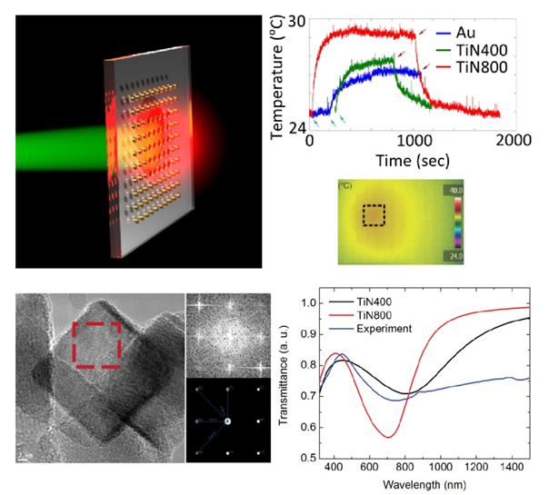
Papers Published:
- U. Guler, S. Suslov, A. V. Kildishev, A. Boltasseva, V. M. Shalaev, Colloidal plasmonic titanium nitride nanoparticles: Properties and applications, Nanophotonics, DOI: 10.1515/nanoph-2015-0017 (2015) (*Invited Research Paper*)
- U. Guler, A. Boltasseva, V. M. Shalaev, Plasmonics on the slope of enlightenment: the role of transition metal nitrides, Faraday Discuss. 178, 71-86 (2015) (*Invited Research Paper*)
- U. Guler, V. M. Shalaev, and A. Boltasseva, Nanoparticle Plasmonics: Going Practical with Transition Metal Nitrides, Materials Today, 18, 227-237 (2015) (*Invited Review Paper*)
- U. Guler, A. Boltasseva, and V. M. Shalaev, Refractory Plasmonics, Science 344, 263-264 (2014)
- U. Guler, J. C. Ndukaife, G. V. Naik, A. G. A. Nnanna, A. V. Kildishev, V. M. Shalaev, and A. Boltasseva, Local Heating with Lithographically Fabricated Plasmonic Titanium Nitride Nanoparticles, Nano Letters 13, 6078-6083 (2013)
- U. Guler, G. V. Naik, A. Boltasseva, V. M. Shalaev, and A. V. Kildishev, Performance Analysis of Nitride Alternative Plasmonic Materials for Localized Surface Plasmon Applications, Appl. Phys. B 107, 285-291 (2012)
- U. Guler, A. Kildishev, A. Boltasseva, and V. Shalaev, Titanium Nitride Nanoparticles for Therapeutic Applications, in CLEO: 2014
- U. Guler, J. C. Ndukaife, G. V. Naik, A. G. A. Nnanna, A. Kildishev, V. M. Shalaev, and A. Boltasseva, Local Heating with Titanium Nitride Nanoparticles, in CLEO: 2013, OSA Technical Digest (online) (Optical Society of America, 2013), QTu1A.2
- U. Guler, G. Naik, A. Boltasseva, V. Shalaev, and A. Kildishev, Nitrides as Alternative Materials for Localized Surface Plasmon Applications, in Frontiers in Optics 2012/Laser Science XXVIII, OSA Technical Digest (online) (Optical Society of America, 2012), FTh4A
Unlocking New Physics and Novel Applications using Nanowire-based Hyperbolic Metamaterials
Contact: Rohith Chandrasekar
Advisors: Dr. Xiangeng Meng, Prof. Alexander Kildishev, Prof. Vladimir Shalaev
Collaborators: Prof. Alexandra Boltasseva, Prof. Alexander Wei, Dr. Yantao Pang (Shandong Jianzhu University)
Short project description:
Hyperbolic metamaterials are a new class of metamaterials that exhibit hyperbolic dispersion, a characteristic that can be applied to achieve exciting phenomena such as subdiffraction imaging, radiative decay engineering, hyperlensing and single-photon sources, to name a few. Hyperbolic metamaterials can be fabricated using two geometries: (1) alternating metal and dielectric layers, or (2) growing metal nanowires in a dielectric host matrix.
In this project, we focus on fabricating highly-ordered, high-quality gold and silver nanowire arrays in an alumina matrix. The samples are grown directly on a glass substrate for ease in characterization and device implementation. Using these new materials, we are currently pushing forward on multiple efforts: (1) measuring lifetime enhancement of dyes and nanodiamonds placed on or embedded in nanowire arrays, (2) studying lasing characteristics of nanowire arrays embedded in laser dyes, and (3) fabricating curved nanowire structures for future studies in hyperlensing and subdiffraction imaging.

Papers Published:
- Y. Pang, R. Chandrasekar, "Cylindrical and spherical membranes of anodic aluminium oxide with highly ordered conical nanohole arrays" Natural Science 7, 232-237 (2015)
Second-Harmonic Generation with Plasmonic Metasurfaces
Primary Contact: Rohith Chandrasekar
Additional Contact: Naresh K. Emani
Advisors:Prof. Alexander Kildishev, Prof. Vladimir Shalaev
Collaborators: Prof. Alexandra Boltasseva; Dr. Alexei S. Lagoutchev, Prof. David R. Smith (Duke University), Dr. Cristian Ciraci (Duke University)
Short project description:
In this project, we would like to directly compare the enhancement provided by electric and magnetic resonances for second harmonic generation (SHG). We study SHG by a metasurface consisting of coupled silver nanostrips that exhibits both electric and magnetic resonance for TM-polarized light. We set the electric resonance at the second harmonic and the magnetic resonance at the fundamental. By tuning the magnetic resonance on and off the fundamental, we can study each resonance individually and study their combined effects. We find that the electric resonance provides twice the enhancement provided by magnetic resonance. We use simulations and fittings to show that SHG by magnetic resonance is inhomogeneously broadened due to its broad tunability.

Papers Published:
- R. Chandrasekar, N. K. Emani, A. Lagutchev, V.M. Shalaev, A.V. Kildishev, C. Ciraci, and D.R. Smith, "Second Harmonic Generation by Metamagnetics: Interplay of Electric and Magnetic Resonances" Frontiers in Optics 2014
- R. Chandrasekar, N. K. Emani, A. Lagutchev, V.M. Shalaev, C. Ciraci, D.R. Smith, and A.V. Kildishev, "Studying the Interplay of Electric and Magnetic Resonance-Enhanced Second Harmonic Generation: Theory and Experiments" CLEO/QELS 2015, San Jose CA.
- R. Chandrasekar, N. K. Emani, A. Lagutchev, V.M. Shalaev, C. Ciraci, D.R. Smith, and A.V. Kildishev, "Second Harmonic Generation by Plasmonic Metasurfaces: Direct Comparison of Electric and Magnetic Resonances" (Submitted to Optical Materials Express Special Optics on Plasmonics)
Near field characterization of plasmonic nanostructures
Contact: Clayton DeVault
Additional Contacts: Paul West, Alexei Lagoutchev
Advisors: Prof. Vladimir Shalaev, Prof. Alexandra Boltasseva
Short project description:
The ability to "see" at the nano-scale is enormously important to the fields of plasmonics and metamaterials. Although the ultimate spatial resolution of a far-field imaging system is limited by diffraction to roughly half the wavelength of the light source, there are several methods to circumnavigate this diffraction limit. Near-Field Scanning Optical Microscopy (NSOM) is a technique that allows resolution well below the natural restriction imposed by diffraction. This is accomplished by maintaining an optical fiber in extremely close proximity (a fraction of the wavelength) to a sample’s surface. At these distances, the optical probe interacts with non-propagating evanescent fields. The spatial resolution is then limited only by the size of the optical fiber’s aperture, which may be as small as 50nm. We utilize this technique to study structures such as nano-antennas, plasmonic waveguides, and metasurfaces. Our NSOM system is capable of operating in reflection, collection, and illumination modes at wavelengths of 532, 633, 785, and 1550 nm.

Papers Published:
- M. D. Thoreson, R. B. Nielsen, P. R. West, A. Kriesch, Z. Liu, J. Fang, A. V. Kildishev, U. Peschel, V. M. Shalaev, A. Boltasseva, Studies of plasmonic hot-spot translation by a metal-dielectric layered superlens, Proc. SPIE, 2011
- DReuben M Bakker, Vladimir P Drachev, Zhengtong Liu, Hsiao-Kuan Yuan, Rasmus H Pedersen, Alexandra Boltasseva, Jiji Chen, Joseph Irudayaraj, Alexander V Kildishev and Vladimir M Shalaev, Nanoantenna array-induced fluorescence enhancement and reduced lifetimes, New Journal of Physics 10, 125022 (2008)
- Reuben M. Bakker, Hsiao-Kuan Yuan, Zhengtong Liu, Vladimir P. Drachev, Alexander V. Kildishev, Vladimir M. Shalaev, Rasmus H. Pedersen, Samuel Gresillon, Alexandra Boltasseva, Enhanced localized fluorescence in plasmonic nanoantennae, Appl. Phys. Lett. 92, 043101 (2008)
- Reuben M. Bakker, Alexandra Boltasseva, Zhengtong Liu, Rasmus H. Pedersen, Samuel Gresillon, Alexander V. Kildishev, Vladimir P. Drachev, and Vladimir M. Shalaev, Near-field excitation of nanoantenna resonance, Optics Express, Vol. 15, Issue 21, pp. 13682-13688 (2007)
- R.M. Bakker, V.P. Drachev, H.-K. Yuan, and V.M. Shalaev, Enhanced transmission in near-field imaging of layered plasmonic structures, Optics Express, v. 12, #16, pp. 3701-3706 (2004)
Chemical synthesis of nanomaterials
Contact: Dr. Swati Pol
Advisors: Prof. Vladimir Shalaev, Prof. Alexandra Boltasseva
Computer modeling of random plasmonic nanostructures
Contact: Jieran Fang
Advisors: Prof. Alexander Kildishev, Prof. Vladimir Shalaev