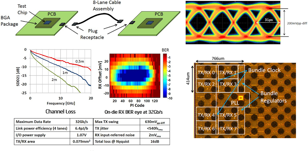
High-Speed IO / Proximity Communication
High-speed Scalable (4-32 Gb/s) Power-Efficient (1-6.3pJ/b) Wireline Link & Reversible Low-Profile Connector for the Next Decade
Imagine the possibilities if USB transfer speed were 10-100 times higher. Or the convenience if all devices used only one connector and only
one kind of universal connector. This breakthrough circuit/system research enables this vision by implementing a dense, low profile converged IO connector.
Along with the connector, the transceiver capable up to 32Gb/s per lane (8 lanes total) is demonstrated. Channel equalization is performed by a combination
of a 3-tap feed-forward equalizer (FFE), single-stage continuous-time linear equalizer (CTLE) and a 6-tap decision feed-forward equalizer (DFE). Collaborative
timing recovery is used to enable lane characterization without degrading jitter performance. Phase error decimation, with a conditional phase detection scheme,
is used to reduce the DFE complexity by 50%. Power consumption over wide range of data rates from 4 to 32Gb/s is reduced by using regulated CMOS clocking with
lane bundling, low swing transmitter with a source-series terminated (SST) driver and a highly reconfigurable receiver with an active inductor CTLE. Adaptivity
is built into the IC to support scalable mufti-standard operation. At a lane data rate of 32Gb/s, over a 0.5m cable with 16dB of loss, a transceiver lane consumes
205mW from a 1.07V supply. The power scales down to 26mW from a 0.72V supply at 8Gb/s, when transmitting over a channel with 8dB loss.
Key Publications : ISSCC 2014, JSSC 2014
Multi-standard High Speed Transmitter with Differential 25.6 Gb/s and Dual-Mode DDR/GDDR5 Operation
A wide range of memory configurations exist in today’s high-speed digital systems to meet platform-specific bandwidth, power, capacity, and cost constraints.
In the near term, DDR4 and GDDR5 are expected to meet the needs of server, client, graphics and mobile platforms. Differential signaling with high-speed serial I/O enhancements
will potentially continue I/O performance scaling for post-DDR4 and future buffered memory solutions. A unified memory interface that can meet the signaling requirements of all
these memory standards offers several benefits: reduced cost and design time, greater platform design flexibility, and a smoother transition from DDR4/ GDDR5 to a high-speed differential
memory interface. This work presents a dualmode TX that supports single-ended (SE) 1.2V-DDR4/1.5V-GDDR5 as well as high-speed differential signaling which is implemented using only
thin-gate-oxide devices in 22nm CMOS. Other key design features include: (a) a DDR4/GDDR5 driver implemented using only active devices (no linearizing resistors), (b) enhanced
voltage-mode driver supply regulation, (c) reconfigurable logic to support pre-emphasis in both TX modes, and (d) low overhead digital clock calibration techniques based on asynchronous
digital sampling (ADS) to improve calibration coverage and accuracy.
Key Publications : ISSCC 2014
Hybrid Mixed-mode High PSRR, Wideband, Fast Settling LDO for High Speed IO Clocking
We developed a hybrid mixed-signal analog/digital LDO that benefits from the virtues of both analog and digital LDO. On the analog side, compared to a PMOS based feedback
loop, a current-source based PMOS provides additional supply rejection over all frequency. A shunt current stealing based (push-pull also possible) feedback loop provides wide bandwidth
(lower capacitance at NMOS gate) rejection. Output dominant pole results in no PSRR peaking and guaranteed stability even under extra parasitic capacitance on regulated node. A digital
feedback loop with dead-band allows sophisticated controller design and fast sampling speeds result in fast settling time, which cannot be achieved with a fully analog LDO.
Key Publications: JSSC 2014
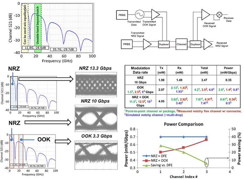
Multi-band (BB + Up converted) Communication through Notchy Wireline Channels
Various forms of discontinuities such as stubs, vias, and wire bonds can result in deep amplitude notches in wireline channels. The data rate for systems operating using such
channels, in the absence of a power-hungry decision-feedback equalizer (DFE), is limited by the lowest notch frequency of the channel. This brief proposes a multiband transceiver system to
overcome this limitation by upconverting part of the data using an on–off keying modulation to avoid operating near the notch frequency and multiplexes it with the original baseband data.
The transceiver system implemented in 45-nm low-power CMOS and shows a 10%–50% increase in data rate with a power saving of 5%–30% over a traditional broadband system employing a DFE in
exemplary channels.
Key Publications: TCAS II 2011