Quantitative RTD Simulation
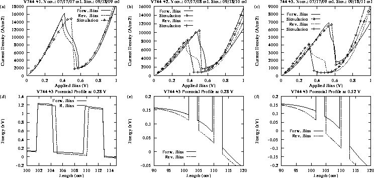
Test matrix of a strained InGaAs/AlAs RTD system. One of the AlAs barriers is increased in thickness by one mono-layer at the time. The nominally symmetric device V744 #1 has nominal well and barrier thicknesses of 30Å/10 mono-layer (ml) and 47Å/16ml, respectively. The devices are symmetrically clad with 20Å/7ml undoped, 500Å low doping (1e18cm-3) and 500Å high doping (5e18cm-3) spacer/contact layers. a-c) Comparison of experimental and simulated I-V's. Forward bias (thicker collector barrier) shows a higher peak current at a higher voltage. d-f) Potential profiles calculated for device #3 in forward and reverse bias for biases 0.28 V and 0.52 V. For comparison we reverse the spatial order of the layers for the reverse bias device. d) 0.28 V bias. The forward bias direction implies a thicker collector barrier. e) Zoom of (d). Reverse bias has a linear potential drop in the well indicating negligible electron charge in the well. Forward bias shows curvature in the well indicating electron accumulation resulting in a potential difference of about 40meV. f) 0.52V bias. Potential difference in the well is about 90meV due to charge accumulation in forward bias. A higher bias must be applied to the RTD to turn off the RTD.
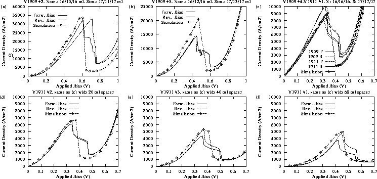
Test matrix of an unstrained InGaAs/InAlAs RTD system. The cladding is the same as described in Figure above. a-c) Variation of the well thickness ((a) 11 ml, (b) 12 ml, (c) 16 ml). c-f) Variation of the undoped spacer layer ((c) 7ml, (d) 20 ml, (e) 40 ml, (f) 68 ml).
These results were published in the Device Research Conference 1997 [P13].