Resonances in the Contacts
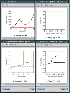
The figure on the left shows four panels:
Top left: Current voltage characteristicTop right: Current density.Bottom left: Conduction band edge with resonances.Bottom right: Transmission coeffcient.
The non-uniform doping profile that is typically used in RTD design produces a float-up of the conduction band edge in the center of the device region. A triangular well will form in the emitter when a bias is applied. This triangular well will locally bind at least one resonance state. This resonance state will interact with the central device resonance state. Effects of this so-called emitter-quasi-bound can be seen in the current density as well as the transmission coefficient. One of the major achievements of the NEMO project was the proper treatment of these emitter quasi-bound states. For more information please see formal publications such as [10,12] A comparison between three different boundary conditions can be found on a different page.
The simulations shown here only illustrate the basic operation of an RTD. Effects such as temperature dependence, charging effects and bandstructure effects are not included here.