Basic RTD (Resonant Tunneling Diode) Operation
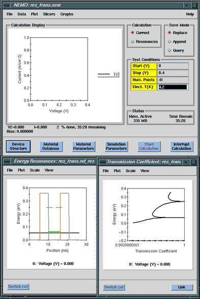
The figure on the bottom shows three panels: Top: RTD Current voltage characteristic at low temperature (4.2K).Bottom left: Conduction band edge with resonances. No charge accumulation included for simplicity.Bottom right: Transmission coeffcient.
The resonances in the center of the device act as a band-pass filter. The position of the resonances is aligned with sharply spiked transmission through the double barrier structure. As the voltage is increased on the collector (right) side the resonances are lowered.
The contacts of the device provide a sea of electrons as indicated by the horizontal lines (Fermi energies). As the resonance (band-pass) is lowered into the sea of electrons on the left, current starts to flow. The current increases until the resonances hits the bottom of the emitter (left side) conduction band edge and no more electrons can be provided by the contact to tunnel through the resonance state. Once the second resonance state dips into the Fermi-sea of electrons, current starts to increase again.
The simulations shown here only illustrate the basic operation of an RTD. The following RTD modeling issues are discussed elsewhere:Introduction to RTDs.Introduction to heterostructures.Animation of the temperature dependence.Basic charge distributions.Animation of the charge development.Animation of the effects of resonances in the contacts.Animation of the different contact treatments.An example of quantitative RTD modeling.A discussion on realistic electron dispersion relations.