Basic charge distributions
In order to inject a significant amout of carriers into the RTD the contacts must be degenerately doped. Typical doping levels are 5e18cm-3. Heavy doping in the central device structure will lead to strong ionized doping scattering and a degradation of the diode peak-to-current ratio. Typical RTD structures have therefore very little doping (no intentional doping) in the central device region (1e15cm-3). The non-uniform doping will result in a non-uniform free carrier distribution even in equilibrium. The free electrons in the contacs will diffuse out into the central device region which contains only few electrons. This diffusion charges the central device region negatively and raises the electrostatic potential to prevent further influx of free electrons. The equilibrium potential profile will be bulged up in the central device region.
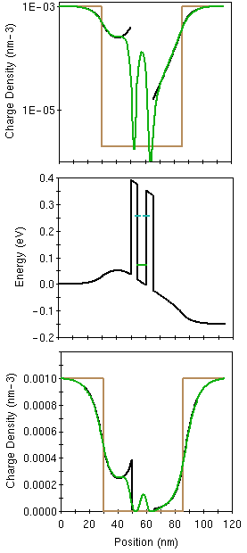
The figure on the left shows three panels: Top: Charge densities (doping profile (brown), semicalssical charge (SC) (black) and quantum mechanical (QM) charge (green) on a logarithmic scale. The unit conversion here is 1e18cm-3=1e-3nm-3.Middle: Conduction band profile and resonance states corresponding to the semi-classical charge distribution.Bottom: Same as top, but on a linear scale.
NEMO can compute semi-classical charge in quasi equilibrium using a semi-classical (Thomas-Fermi) approach. It is well known that this approach over-estimates the charges at barriers. Also it depends strongly on the definition of the Fermi energy.
A quantum mechanical charge computation (Hartree self-consistency) shows the well behaved charge distribution at the interface (note the symmetry of the emitter-quasi-bound state in the charge distribution in the emitter!) and it exhibits a significant charge component in the central device structure.
The dramatic effects of quantum mechanical charge accumulation in the central device region is discussed in the context of quantitative RTD modeling and an animation of the charge development.