Zhengping Jiang's Biography
EDUCATION
Tianjin University, Tianjin, China
B.S. in Electronic Science and Technology July 2008
Purdue University, West Lafayette, USA
M.S. in Electrical and Computer Engineering May 2011
Ph.D in Electrical and Computer Engineering May 2011 to December 2015
RESEARCH INTERESTS
Zhengping Jiang joined Professor Klimeck's research group in August 2008 at Purdue University. He is a PhD student in this group. His research focuses on quantum transport in untra-scaled transistors and electronic properties of Si quantum well with application in Quantum Computing. Zhengping is using NEMO 3-D as a primary vehicle for modeling and simulation and he is now involved in development of NEMO 5.
PROFESSIONAL EMPLOYMENT
Sr. Engineer, Samsung Semiconductor Inc. Jan. 2016 to present
Research Assistant, ECE, Purdue University Aug. 2008 to Dec. 2015
Research focuses: Atomistic nanoelectronic simulation, quantum transport in untra-scaled transistors, high performance computation, peta-scale computing applications development.
Supervisor: Professor Gerhard Klimeck
Engineer Intern, Samsung Semiconductor Inc. Jul. 2015 to Dec. 2015
Manager: Jing Wang
Co-Op Engineer, GLOBALFOUNDRIES Inc. Jun. 2013 to Aug. 2013
Tight-binding modeling of III-V FinFET. Effects of alloy scatteirng.
Mentors: Bejhtash Behin-Aein, Zoran Krivokapic
Summer Internship, IBM T. J. Watson Research Center Jun. 2012 to Aug. 2012
Tight-binding modeling of metal insulator transition in piezoresistive material SmSe. Quantum transport in Piezoelectronic Transistor.
Mentors: Glenn Martyna, Dennis Newns
Zhengping has a contributor web page on nanoHUB.org.
During his tenure in the Klimeck group he worked on the following research projects:
RESEARCH PROJECTS:
Develop all-purpose Nanoelectronics Simulation Toolkit NEMO 5 (since Fall, 2010)[J257][J204][P168]
- Modular design, multi-level parallelization, atomistic structure towards multimillion-atom simulation, ~20 co-developers.
- Program with C++ primarily and have experiences on MPI and numerical packages.
- Use NEMO5 to power online simulation tools in nanoHUB.org and conduct scientific research projects.
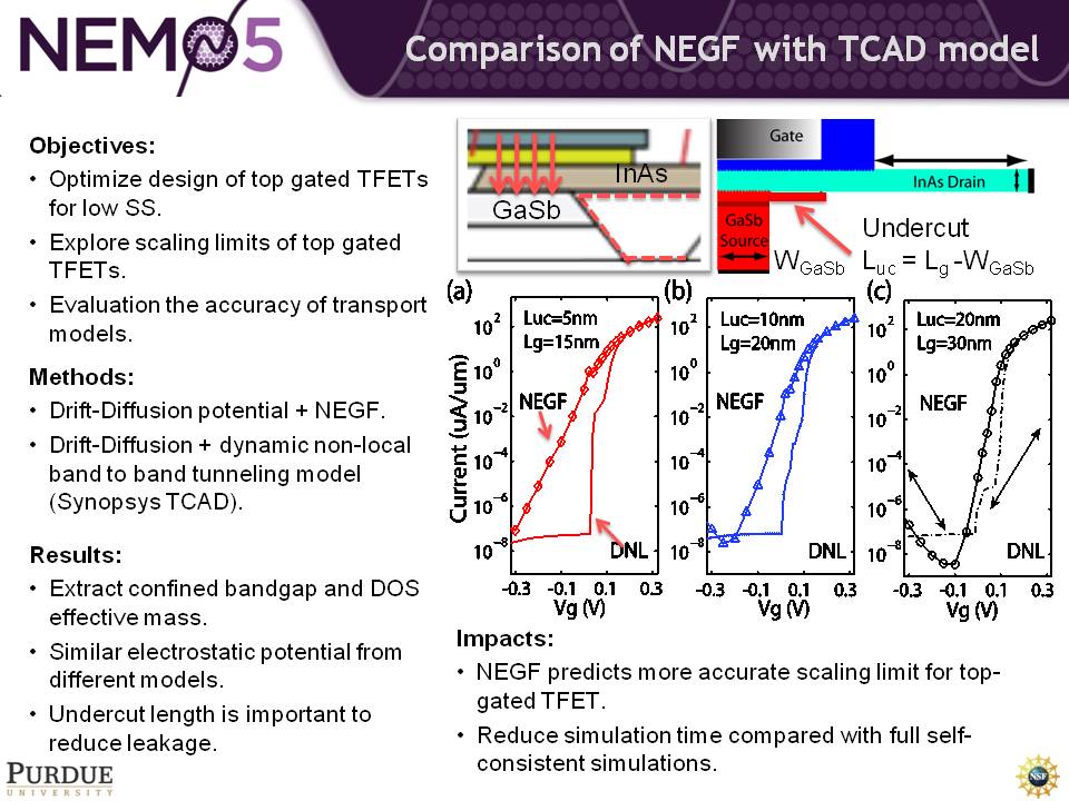
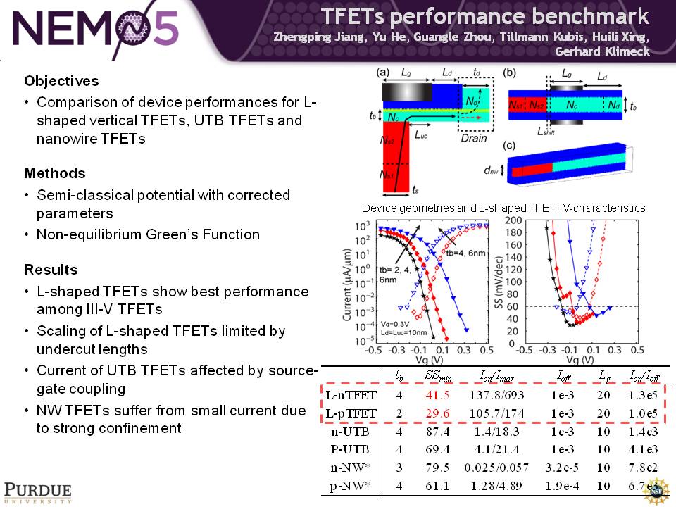
Quantum Transport Modeling of Ultra-scaled Transistors (MIND/NRI funded / joined in April, 2011)[C386][C385][C358][P173][J260][J206][B6]
- Explore ultimate scalability of band to band tunneling diode and Tunneling FET.[PPT1 PPT2]
- Deliver insight on fundamental effects that limit device performance (phonon scattering, bandgap engineering, impurity and defect).[P171]
- Collaborate with experimental groups to provide guidelines for future fabrication.
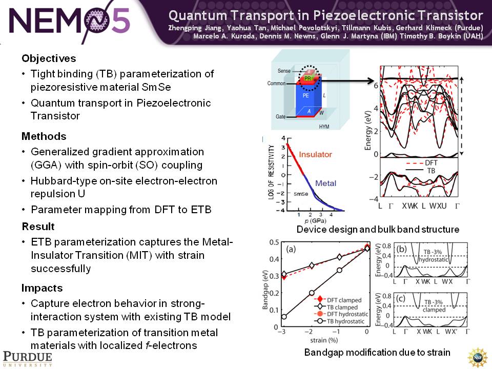
Tight-binding simulation of Piezoelectronic Transistors[J195][J187][J225][C398][PPT]
- Ab initio study on pressure-induced Metal Insulator Transition.
- Tight-binding parameterization of intermediate valence compound SmSe.
- Quantum transport in strong correlated electron systems with f-band electrons.
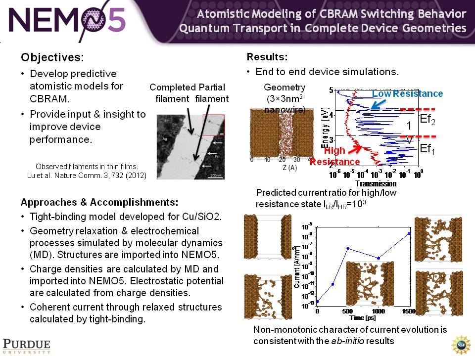
Simulation of Resistive Random Access Memory (RAM)[PPT]
- Modeling of filamentary conduction in Cu/SiO2 based CBRAM.
- Tight binding parameterization of copper and silicon dioxide for electronic transport.
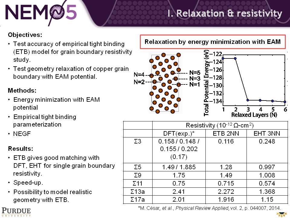
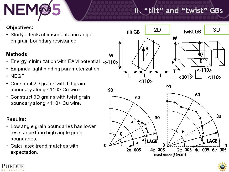
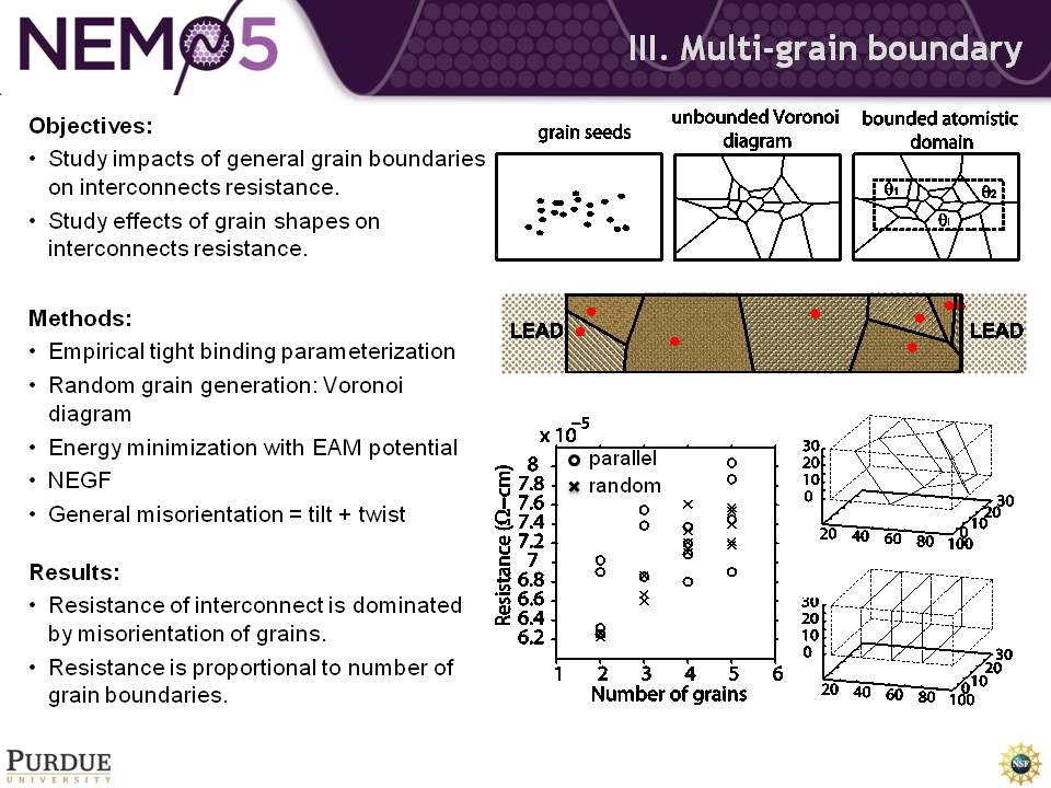
Simulation of grain boundary resistance in ultra scaled Cu interconnect[PPT]
- Energy minimization with interatomic EAM potential.
- Environmental dependent tight binding model.
- Coherent grain boundary and random grain boundary.
Electronic Transport in ultra-scaled MOSFET[PPT]
- Modeling of advanced MOSFETs under 14/10nm technology nodes.[J231]
- Effects of alloy scattering in InGaAs MOSFETs.


Simulation of quantum transport in III-V Resonance Tunneling Diode(RTD)
- RTD simulation tool with NEGF by C and Matlab mixed programming.
- Complex eigenvalue resonance finder.
- Bandstructure effects in III-V material on RTD transport properties by emperical tight-binding simulation.
Electronic bandstructure of Si/SiGe and valley splitting in Si quantum wells[J171][C343][C306][P138][P115]
- Valley degeneracy in (011) Si quantum wells
- Effects of disorder on valley splitting in (001) Si/SiGe quantum wells
- Band unfolding algorithm for disordered material system