Laser Strain Engineering
Laser Strain Engineering
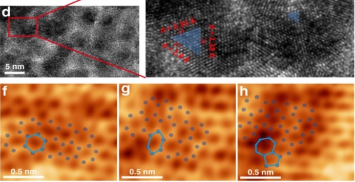
Straining nanomaterials to break their lattice symmetry is perhaps the most efficient approach toward realizing bandgap tunability. A modulated inhomogeneous local asymmetric elastic–plastic straining is reported that utilizes GPalevel laser shocking at a high strain rate (dε/dt) ≈ 106–107 s−1, with excellent formability, inducing tunable bandgaps in graphene, and nanoscale electro-optical property changes in many 2D materials and their heterostructures.
References:
-
M. Motlag, P. Kumar, Y. Hu, S. Jin, J. Li, J. Shao, X. Yi, Y.H. Lin, J. Walrath, L. Tong, X. Huang, R.S. Goldman, L. Ye, G.J. Cheng, “Asymmetric 3D elastic-plastic strain-modulated electron energy structure in monolayer graphene by laser shocking” , Advanced Materials, (2019), https://doi.org/10.1002/adma.201900597
-
Y Wang, S Yao, P Liao, S Jin, Q Wang, MJ Kim, GJ Cheng, W Wu, “Strain-engineered anisotropic optical and electrical properties in two-dimensional chiral-chain tellurium", Advanced Materials, (2020), https://doi.org/10.1002/adma.202002342
-
T. K. Sahu, M. Motlag, A. Bandyopadhyay, G.J. Cheng, P. Kumar, "2+δ dimensional materials via Atomistic Z-welding", Advanced Science, (2022).
-
Y. Hu, F. Zhang, M. Titze, B. Deng, H. Li, and G.J. Cheng, “Straining effects in MoS2 monolayer on nanostructured substrates: temperature-dependent photoluminescence and exciton dynamics”, Nanoscale, 10(12), (2018), DOI: 10.1039/C8NR00332G
-
Maithilee Motlag, Yaowu Hu, Lei Tong, Xinyu Huang, Lei Ye, Gary J. Cheng, “Laser shocking induced nanoscale kink-bands in WSe2 2D crystals”, ACS Nano, (2019).https://doi.org/10.1021/acsnano.9b04705.
-
Hu, Y; Li, J; Tian, J; Xuan, Y; Deng, B; Lim DT; McNear, K; Chen, Y; Yang, C; Cheng, GJ, "Parallel nanoshaping of brittle semiconductor nanowires for strained electronics", Nano Letters, (2016).DOI: 10.1021/acs.nanolett.6b03366
-
J Li, TF Chung, YP Chen, GJ Cheng, “Nanoscale Strainability of Graphene by Laser Shock Induced 3D Shaping", Nano Letters, (2012) Doi:10.1021/nl301817t.
-
P Kumar, M Motlag, J Liu, Y Hu, L Ye, J Irudayaraj, GJ Cheng, "Laser shock tuning dynamic interlayer coupling in graphene moiré superlattices", Nano Letters, (2018), DOI: 10.1021/acs.nanolett.8b03895.
-
Chunpeng Song, Huanrui Yang, Feng Liu, Gary J. Cheng, "Quantum Dots enabled Perovskite Thin Film with Enhanced Crystallization, Stability, Carrier diffusion via Pulsed Laser Nanoengineering", Advanced Materials Interfaces, (2020).DOI: 10.1002/admi.202001021.
-
Yixiu Wang, Shengyu Jin, Qingxiao Wang, Min Wu, Shukai Yao, Peilin Liao, Moon J. Kim, Gary J. Cheng, Wenzhuo Wu, "Parallel nanoimprint forming of one-dimensional chiral semiconductor for strain-engineered optical properties", Nano-Micro Letters, (2020). DOI : 10.1007/s40820-020-00493-3
-
Q. Nian, L. Gao, Y. Hu, B. Deng, J. Tang, G.J. Cheng, "Graphene/PbS-Quantum Dots/Graphene Sandwich Structures Enabled by Laser Shock Imprinting for High Performance Photodetectors", ACS Applied Materials & Interfaces, (2017), 9(51):44715-44723. doi: 10.1021/acsami.7b14468.
-
DC Branco, GJ Cheng, "A strategy for 2D MXenes as thermal management materials by laser shock Nanoshaping", Journal of Physics: Materials (2023).
-
X Huang, L Zhang, L Tong , Z Li, Z Peng, R Lin, K-H Xue, H Dai, H Cheng, DC Branco, J-B Xu, J-B Han, GJ Cheng, X Miao, L Ye, "Manipulating Exchange Bias in 2D Magnetic Heterojunction for High-performance Robust Memory Applications", Nature Communication, 14: 2190 (2023).https://doi.org/10.1038/s41467-023-37918-7