Current projects
- Quantum Nanophotonics with 2D Materials
- On-Chip Photonics and High Speed Optical Modulators
- Machine learning assisted optimization of photonic/plasmonic metastructures
- Machine learning assisted quantum photonics
- Quantum Nanophotonics with 2D Materials
- On-Chip Photonics and High Speed Optical Modulators
- Plasmon-induced magnetic-field-assisted nanomagnet switching with femtosecond laser pulses
- Epsilon-near-zero (ENZ) and Nonlinear Optics
- Mapping the nanoscale energy distributions of plasmonic hot-carriers
- Quantum Nano-optics
- MURI: Near-Field Radiative Heat Transfer between Nanostructured Materials
- Robust Vivid Plasmonic Color Printing
- Transdimensional Plasmonic Materials
- Refractory Plasmonics
- Novel Optics with Metasurfaces
- Nanolasers
- Alternative Plasmonic Materials
- Plasmonics with Graphene & Beyond
- Integrated Nanophotonic Devices with Alternative Materials
- *** Completed projects ***
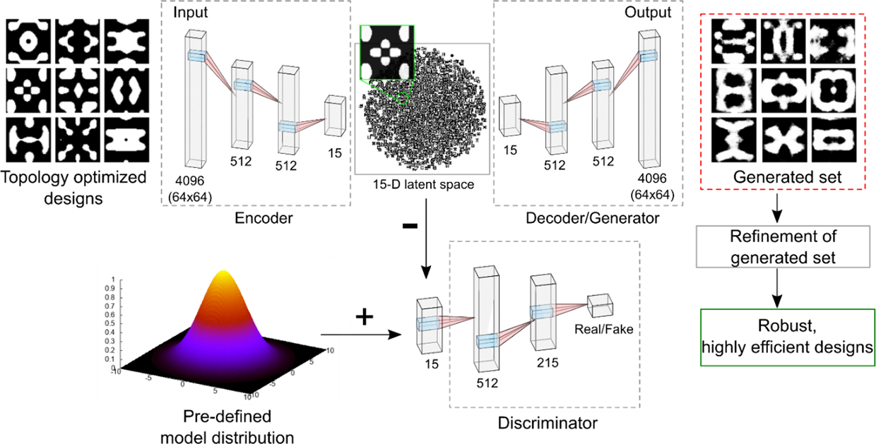
Machine learning assisted optimization of photonic/plasmonic meta-structures
Primary Contact: Zhaxylyk Kudyshev
Additional Contact: Omer Yesilyurt
Advisors: Profs. Alexandra Boltasseva, Vladimir Shalaev, Alexander Kildishev
Short project description:
The realization of practical optical structures and devices is an inherently complex problem due to multi-faceted requirements with manifold stringent constraints on optical performance, materials, scalability, and experimental tolerances. These multiple requirements inevitably open up an enormously large optimization space. Despite the complexity of the available parametric space, almost all nanophotonic structures to date are designed either intuitively or based on a priori selected topologies, and by adjusting a very limited number of parameters (e.g., the periodicity, the trivial geometrical shapes, and dimensions of the resonant elements). Such intuition-based models are only useful for ad hoc needs and have limited applicability and predictive power. Exhaustive parameter sweeps are often done “by hand.” Since comprehensive searches in hyper-dimensional design space is extremely resource intensive, multi-objective optimization has so far been prohibitive.
The innovatory field of the inverse design has recently been transforming conventional nanophotonics by allowing for the discovery of unorthodox optical structures via computer algorithms. The realization of these computer generated designs requires truly new approaches combined with already established diverse optimization and sensitivity methods such as genetic algorithms and different variations of the adjoint method. Within this project, we seek to develop ‘physics-driven’ machine learning optimization frameworks for rapid optimization of meta-structures with extreme properties. Specifically, we propose to combine conventional optimization algorithms with generative networks (GANs and autoencoders) for addressing different interdisciplinary problems.
[1] Zh. A. Kudyshev, A. V. Kildishev, V. M. Shalaev, A. Boltasseva, Machine-learning-assisted global optimization of photonic devices, Nanophotonics, accepted (arXiv:2007.02205)
[2] W. Ma, Z. Liu, Zh. A. Kudyshev, A. Boltasseva, W. Cai, Y. Liu, Deep learning for the design of photonic structures, Nature Photonics, 2020, https://www.nature.com/articles/s41566-020-0685-y
[3] Zh. A. Kudyshev, A. V. Kildishev, V. M. Shalaev, A. Boltasseva, Machine-learning-assisted metasurface design for high efficiency thermal emitter optimization, Applied Physics Reviews,Vol.7,2, 021407 (2020), Featured Article, AIP Scilights
[4] Zhaxylyk A. Kudyshev, Alexander V. Kildishev, Vladimir M. Shalaev, and Alexandra Boltasseva "Deep learning assisted photonics", Proc. SPIE 11461, Active Photonic Platforms XII, 114610C (20 August 2020); https://doi.org/10.1117/12.2567198
[5] Zhaxylyk A. Kudyshev, Simeon Bogdanov, Alexander V. Kildishev, Alexandra Boltasseva, and Vladimir M. Shalaev "Machine learning assisted plasmonics and quantum optics", Proc. SPIE 11460, Metamaterials, Metadevices, and Metasystems 2020, 1146018 (20 August 2020); https://doi.org/10.1117/12.2567310
[6] Zhaxylyk A. Kudyshev, Alexander V. Kildishev, Vladimir M. Shalaev, and Alexandra Boltasseva, Machine-learning-assisted topology optimization for highly efficient thermal emitter design, in Conference on Lasers and Electro-Optics, OSA Technical Digest (Optical Society of America, 2019), paper FTh3C.2.
Machine learning assisted quantum photonics
Primary Contact: Zhaxylyk Kudyshev
Advisors: Profs. Alexandra Boltasseva, Vladimir Shalaev, Alexander Kildishev
Collaborators: Prof. Simeon Bogdanov
Short project description:
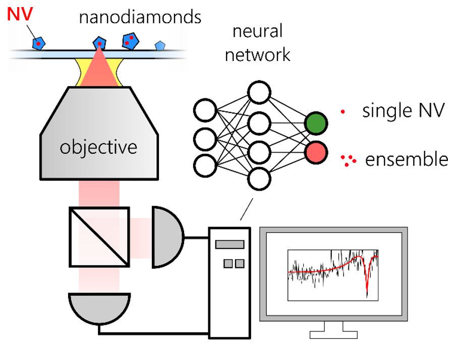
Integrated quantum photonics has recently emerged as one of the key enablers of quantum information science and technology. Typically, quantum photonic circuits are realized using nonlinear sources of single photons that operate probabilistically. These do not allow for the generation of large multi-photon states. Alternatively, solid-state quantum emitters have recently offered near-ideal single-photon emission characteristics. Successful implementation of quantum photonic circuits depends crucially on the selection of quantum emitters from a large inhomogeneous set. In particular, efficient and rapid identification of bright, stable single-photon emitters with fast emission rates, high quantum yield, and narrow optical linewidth is critical. This project aims to develop ML-assisted quantum material characterization and metrology measurement techniques.
Recently, we have developed a method of applying advanced ML and deep learning algorithms to autocorrelation measurements of quantum emission, the back-bone of the quantum optical characterization, and demonstrated rapid identification of the “purity” of a quantum emitter (in our case, nitrogen-vacancy centers in nanodiamonds) with unparalleled speed. The new ML-based approach enables a hundredfold speedup and can be applied to the next generation of single-photon sources and future quantum materials metrology.
Within this project, we are combining quantum optics with a machine/deep leaning algorithm to achieve dramatic speed-up and high precision in the broad range of quantum characterization and quantum metrology applications. One of the directions of the project is ML assisted characterization techniques of single-photon sources based on 2D material platforms and solid state. Yet another direction is the development of ML assisted frameworks for sensing and imaging applications.
[1] Zh. A. Kudyshev, S. Bogdanov, T. Isacsson, A. V. Kildishev, A. Boltasseva, V. M. Shalaev, Rapid classification of quantum sources enabled by machine learning, Advanced Quantum Technologies, DOI: 10.1002/qute.202000067, (arXiv:1908.08577), Highlighted by AAAS EurekAlert, Phys.org
[2] Zhaxylyk A. Kudyshev, Simeon Bogdanov, Alexander V. Kildishev, Alexandra Boltasseva, and Vladimir M. Shalaev "Machine learning assisted plasmonics and quantum optics", Proc. SPIE 11460, Metamaterials, Metadevices, and Metasystems 2020, 1146018 (20 August 2020); https://doi.org/10.1117/12.2567310
[3] Zhaxylyk A. Kudyshev, Simeon Bogdanov, Theodor Isacsson, Alexander V. Kildishev, Alexandra Boltasseva, and Vladimir M. Shalaev "Machine learning-assisted classification of quantum emitters (Conference Presentation)", Proc. SPIE 11295, Advanced Optical Techniques for Quantum Information, Sensing, and Metrology, 112950N (10 March 2020); https://doi.org/10.1117/12.2545404
[4] Z. Kudyshev, S. Bogdanov, T. Isacsson, A. V. Kildishev, A. Boltasseva and V. M. Shalaev, "Merging Machine Learning with Quantum Photonics: Rapid Classification of Quantum Sources," 2020 Conference on Lasers and Electro-Optics (CLEO), San Jose, CA, USA, 2020, pp. 1-2.
Quantum Nanophotonics with Two Dimensional Materials
Primary Contacts:
Xiaohui Xu,
Dr. Demid Sychev
Additional Contacts:
Zach Martin,
Dr. Alexander Senichev,
Dr. Alexei S. Lagoutchev
Advisors:
Prof. Alexandra Boltasseva,
Prof. Vladimir Shalaev
Collaborators: Prof. Yong Chen, Prof. Simeon Bogdanov, Prof. Igor Aharonovich, Andres E Llacsahuanga Allcca
Short project description:
Building large quantum communication and computation systems remain very challenging. A big step towards this goal would be the creation of deterministic sources of indistinguishable single photons which can operate at room temperature. Two dimensional (2D) materials and van der Waals crystals, such as hexagonal boron nitride (hBN) and Transition metal dichalcogenide (TMDC) possess unique optoelectronic and photonic properties. Specifically, single photon emission has been observed in various types of 2D materials, making them promising as emerging platforms for quantum sensing, quantum computing, etc. Their two-dimensional nature provides unparalleled advantages for on-chip integration and high-sensitivity applications.
While room-temperature, bright single photon emission has been observed in hBN, the origin of these quantum emitters remains unknown. In this project, we use scanning transmission electron microscopy (STEM) to investigate atomic structure of quantum emitters in hBN, with sub-angstrom resolution. We also explore the possibility to create/engineer quantum defects in hBN deterministically with the electron beam in STEM. Experiments will be combined with ab initio simulations to get a better understanding of those atomic defects in hBN.
Single photon emission in TMDCs comes from either in-layer localized excitons or interlayer excitons. The latter have attracted more interest due to the rich physics and dynamics enabled by the tunable interlayer alignments. In this project, we will investigate and enhance single photon emission from interlayer excitons with plasmonic cavities. Thanks to the out-of-plane optical dipole moment of interlayer excitons, a deterministic narrow-gap plasmonic nanocavity could be assembled, making it possible to achieve ultrabright quantum emission. A similar plasmonic cavity design will also be used to enhance emission from hBN. The ultimate goal of this project is to obtain single photon emitters that generate indistinguishable photons at room temperature with the help of plasmonics.

Papers Published:
- D. Wang, A. E. L. Allcca, T.-F. Chung, A. V. Kildishev, Y. P. Chen, A. Boltasseva & V. M. Shalaev, Enhancing the graphene photocurrent using surface plasmons and a p-n junction, Nature - Light Sci Appl, 9, 126 (2020)
- Jieran Fang, Di Wang, Clayton T. DeVault, Ting-Fung Chung, Yong P. Chen, Alexandra Boltasseva, Vladimir M. Shalaev, and Alexander V. Kildishev, Enhanced Graphene Photodetector with Fractal Metasurface, Nano Lett., v. 17, no. 1, pp. 57–62 (2017)
On-Chip Photonics and High Speed Optical Modulators
Primary Contact: Soham Saha
Collaborator: The Leuthold Group, ETH
Advisors: Prof. Vladimir Shalaev, Prof. Alexandra Boltasseva
Optoelectronics – the ultrafast processing of signals on a chip - by combining the compactness of electronics with the bandwidth of photonics, is the key to driving computational speeds beyond the limits of Moore’s Law. Plasmonics or metal optics is key to achieving this. Surface plasmons are collective oscillations of electrons that emanate when light strikes the surface of a metal under the right conditions. These oscillations have large wavevectors and can confine light beyond the diffraction limit, making it possible to build optical devices that confine light into nanometer-scale dimensions, well beyond the diffraction limit. This project serves to design ultrafast optical modulators with cheap, industry-compatible materials, namely transition metal nitrides and transparent conducting oxides [1]. Titanium nitride, a low-loss, CMOS-compatible material, has been demonstrated to outperform gold in long-range plasmonic waveguide configurations [2]. Electroabsorption modulators with transparent conducting oxides can be used to make ultra-compact modulators on silicon chips [3]. Emerging technologies such has organic electrooptic polymers can also be used to attain ultra-low loss, hybrid plasmonic modulators that transfer data at high-speeds [4]. The findings of this project will benefit the design of low-loss, high-speed on-chip modulators made with fabrication friendly, industry compatible materials.
References:
[1] N. Kinsey, M. Ferrera, V. M. Shalaev, and A. Boltasseva, Examining nanophotonics for integrated hybrid systems: a review of plasmonic interconnects and modulators using traditional and alternative materials [Invited], JOSA B, 32, 121-142 (2015); https://doi.org/10.1364/JOSAB.32.000121
[2] S. Saha, A. Dutta, N. Kinsey, A. V. Kildishev, V. M. Shalaev, and A. Boltasseva, On-Chip Hybrid Photonic-Plasmonic Waveguides with Ultrathin Titanium Nitride Films, ACS Photonics 5 (11), 4423–4431 (2018,); https://doi.org/10.1021/acsphotonics.8b00885
[3] Babicheva, V. E.; Kinsey, N.; Naik, G. V.; Ferrera, M.; Lavrinenko, A. V.; Shalaev, V. M.; Boltasseva, A. Towards CMOS-Compatible Nanophotonics: Ultra-Compact Modulators Using Alternative Plasmonic Materials. Opt. Express 2013, 21 (22), 27326. https://doi.org/10.1364/OE.21.027326.
[4] Haffner, C.; Chelladurai, D.; Fedoryshyn, Y.; Josten, A.; Baeuerle, B.; Heni, W.; Watanabe, T.; Cui, T.; Cheng, B.; Saha, S.; Elder, D. L.; Dalton, L. R.; Boltasseva, A.; Shalaev, V. M.; Kinsey, N.; Leuthold, J. Low-Loss Plasmon-Assisted Electro-Optic Modulator. Nature 2018, 556 (7702), 483–486. https://doi.org/10.1038/s41586-018-0031-4.
Plasmon-induced magnetic-field-assisted nanomagnet switching with femtosecond laser pulses
Primary Contact: Aveek Dutta
Collaborators: Prof. Ernesto Marinero (Purdue), Prof. Vladimir Belotelov (Russian Quantum Center), Prof. Arata Tsukamoto (Nihon University) and Prof. Aleksei V. Kimel (Radboud University)
Advisors: Prof. Vladimir Shalaev, Prof. Alexandra Boltasseva
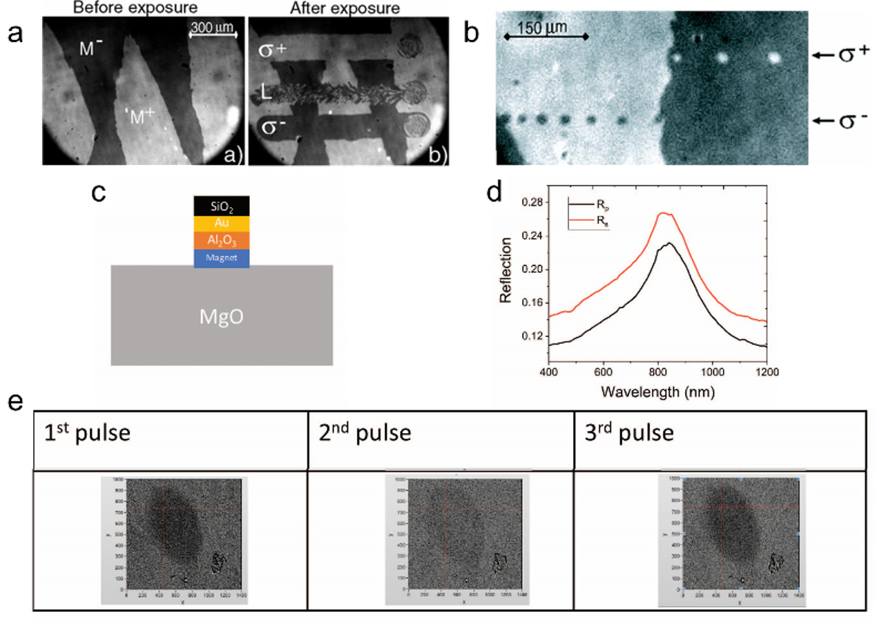
Background: The first demonstration of ultrafast demagnetization with femtosecond (fs) laser pulses was done by Beaurepaire et in in 1996 using a Ni film [1]. Since then the field of ultrafast dynamics in magnetic materials induced by fs laser pulses has been extensively studied both theoretically and experimentally [2]. In this regard, the phenomenon of All Optical Magnetization Switching, or AOMS, deserves a special mention. Figures (a) and (b) highlighting this phenomenon are taken from the work by Stanciu et al [3]. Figure (a)-before exposure shows a ferrimagnetic GdFeCo layer with out-of-plane magnetization in two opposite orientations as depicted by the dark and white areas. Figure (a)-after exposure shows that, depending on its helicity, a circularly polarized 800 nm 100 fs laser pulse can switch the magnetization of one domain while leaving the other un-affected (σ+ and σ- are right and left circularly polarized light respectively). The linearly polarized light L however leads to a random magnetization of the GdFeCo layer. Figure (b) shows that even a single pulse of circularly polarized laser light can reverse the magnetization of the illuminated area. It was later shown that heating of the magnetic material due to the fs laser pulse illumination plays a crucial role in the magnetization reversal of GdFeCo [4,5]. So one could achieve magnetization reversal in GdFeCo even with linearly polarized light. Therefore, enhancing light absorption in GdFeCo should make this magnetization reversal process more energy efficient. This can be achieved by plasmonics.
Research: Figure (c) shows the schematic of the fabricated nanostructure which consists of GdFeCo nanomagnet and Au plasmonic resonator. The entire stack configuration is: MgO substrate / 20 nm Si3N4 / 5 nm Gd31Fe60.4Co8.6 / 3 nm Si3N4 / 5 nm Al2O3 / 30 nm Au / 20 nm SiO2. Figure (d) shows the reflection measurements performed on a nanodisk array of this stack with 250 nm diameter and 400 nm period. The black and red curves are for p and s polarized light respectively. All measurements were done at 20° angle of incidence. The peak in the reflection data corresponds to a plasmon resonance. It was verified with simulations (using COMSOL Multiphysics) that the plasmon resonance corresponds to an increased absorption in the GdFeCo nanomagnet. The fabricated array was illuminated with 100 fs 800 nm linearly polarized light at a fluence of 5.47mJ/cm2. Figure (e) shows the results of our experiment. Following the first laser pulse, the dark area shows the portion of the nanodisk array where GdFeCo magnetization reversed. The second pulse, re-aligns the magnetization in the original direction. The third pulse has a similar effect as the first one. This shows reversible magnetization switching for the nanodisk array. No such switching was observed at the given fluence in an array without the Au plasmonic resonator. This shows that the Au plasmonic resonator increases light absorption and therefore can switch the GdFeCo magnetization at fluences where the GdFeCo nanomagnet by itself won’t switch. It should be noted that a 3mT magnetic field needed to be applied in order to assist the reversible switching of the GdFeCo nanomagnet coupled to Au plasmonic resonator.
References:
[1] E. Beaurepaire, J.-C. Merle, A. Daunois, and J.-Y. Bigot, Phys. Rev. Lett. 76, 4250 (1996)
[2] A. Kirilyuk, A. V Kimel, and T. Rasing, Philos. Trans. A. Math. Phys. Eng. Sci. 369, 3631 (2011)
[3] C. D. Stanciu, F. Hansteen, A. V. Kimel, A. Kirilyuk, A. Tsukamoto, A. Itoh, and T. Rasing, Phys. Rev. Lett. 99, 1 (2007)
[4] I. Radu, K. Vahaplar, C. Stamm, T. Kachel, N. Pontius, H. A. Dürr, T. A. Ostler, J. Barker, R. F. L. Evans, R. W. Chantrell, A. Tsukamoto, A. Itoh, A. Kirilyuk, T. Rasing, and A. V Kimel, Nature 472, 205 (2011)
[5] J. H. Mentink, J. Hellsvik, D. V. Afanasiev, B. A. Ivanov, A. Kirilyuk, A. V. Kimel, O. Eriksson, M. I. Katsnelson, and T. Rasing, Phys. Rev. Lett. 108, 057202 (2012)
[6] A. Dutta, A. V. Kildishev, V. M. Shalaev, A. Boltasseva, and E. E. Marinero, Surface-plasmon opto-magnetic field enhancement for all-optical magnetization switching, Opt. Mater. Express 7(12), 4316-4327 (2017)
Epsilon-near-zero (ENZ) and Nonlinear Optics
Primary Contact: Soham Saha
Secondary Contacts: Zhaxylyk Kudyshev, Mustafa Ozlu
Collaborators: Prof. Daniele Faccio (Glasgow University), Marcello Ferrera, Heriot-Watt University
Advisors: Prof. Vladimir Shalaev, Prof. Alexandra Boltasseva
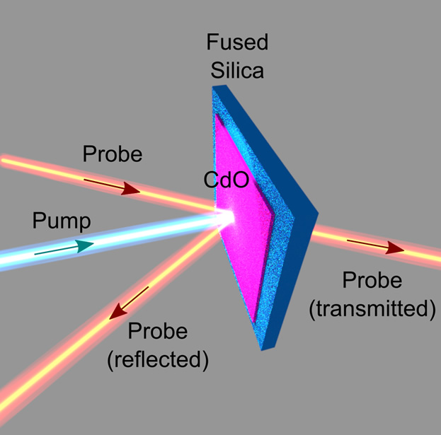
Many extraordinary optical phenomena are enhanced in the epsilon-near-zero (ENZ) regime - the wavelength regime where the complex permittivity of a material is near zero. The slow-light interactions in this regime increase light-matter interactions, bolstering phenomena such as enhanced nonlinearities [1], ultrafast reflection modulation [2], and emitter radiation engineering [3]. Transparent conducting oxides are natural homogeneous ENZ media and they exhibit extremely low-index behavior needed to realize the full potential of extraordinary nonlinear optics for photonics [4]. In this project, we investigate largely unexplored nonlinear optical phenomena in near-zero-index materials, enhanced by the extreme light-matter interaction resulting from the slow-light effect, without a need for complex nanostructure fabrication. Furthermore, the optical properties of these materials can be tuned by doping, thus enabling a great level of control over both the ENZ wavelength and the switching times [5]. We utilize low-loss transparent conducting oxides (TCOs) as homogeneous low index materials with the low-index region in the technologically relevant telecommunication spectrum [6]. We experimentally demonstrate nonlinear effects such as negative refraction [7] and broadband wavelength shifts [8] near the epsilon near zero region in aluminum-doped zinc oxide and tin-doped indium oxide. We also establish theories to better understand and predict the observed nonlinear enhancements. The findings of our research will enable the design of fast, low-loss, and efficient devices for optical modulation, beam steering, and optical isolator design.
References:
[1] Caspani, L.; Kaipurath, R. P. M.; Clerici, M.; Ferrera, M.; Roger, T.; Kim, J.; Kinsey, N.; Pietrzyk, M.; Di Falco, A.; Shalaev, V. M.; Boltasseva, A.; Faccio, D. Enhanced Nonlinear Refractive Index in ϵ -Near-Zero Materials. Phys. Rev. Lett. 2016, 116 (23), 233901. https://doi.org/10.1103/PhysRevLett.116.233901.
[2] Kinsey, N.; DeVault, C.; Kim, J.; Ferrera, M.; Shalaev, V. M.; Boltasseva, A. A. Epsilon-near-Zero Al-Doped ZnO for Ultrafast Switching at Telecom Wavelengths. Optica 2015, 2 (7), 616–622. https://doi.org/10.1364/OPTICA.2.000616.
[3] Kinsey, N.; DeVault, C.; Boltasseva, A.; Shalaev, V. M.; DeVault, C.; Boltasseva, A.; Shalaev, V. M. Near-Zero-Index Materials for Photonics. Nat. Rev. Mater. 2019, 4 (12), 1–19. https://doi.org/10.1038/s41578-019-0133-0.
[4] Kim, J.; Dutta, A.; Naik, G. V.; Giles, A. J.; Bezares, F. J.; Ellis, C. T.; Tischler, J. G.; Mahmoud, A. M.; Caglayan, H.; Glembocki, O. J.; Kildishev, A. V.; Caldwell, J. D.; Boltasseva, A.; Engheta, N. Role of Epsilon-near-Zero Substrates in the Optical Response of Plasmonic Antennas. Optica 2016, 3 (3), 339. https://doi.org/10.1364/OPTICA.3.000339.
[5] Saha, S.; Diroll, B. T.; Shank, J.; Kudyshev, Z.; Dutta, A.; Chowdhury, S. N.; Luk, T. S.; Campione, S.; Schaller, R. D.; Shalaev, V. M.; Boltasseva, A.; Wood, M. G. Broadband, High‐Speed, and Large‐Amplitude Dynamic Optical Switching with Yttrium‐Doped Cadmium Oxide. Adv. Funct. Mater. 2019, 1908377. https://doi.org/10.1002/adfm.201908377.
[6] Naik, G. V; Kim, J.; Boltasseva, A. Oxides and Nitrides as Alternative Plasmonic Materials in the Optical Range [Invited]. Opt. Mater. Express 2011, 1 (6), 1090. https://doi.org/10.1364/OME.1.001090.
[7] Vezzoli, S.; Bruno, V.; Devault, C.; Roger, T.; Shalaev, V. M.; Boltasseva, A.; Ferrera, M.; Clerici, M.; Dubietis, A.; Faccio, D. Optical Time Reversal from Time-Dependent Epsilon-Near-Zero Media. Phys. Rev. Lett. 2018, 120 (4), 043902. https://doi.org/10.1103/PhysRevLett.120.043902.
[8] Khurgin, J. B.; Clerici, M.; Bruno, V.; Caspani, L.; DeVault, C.; Kim, J.; Shaltout, A.; Boltasseva, A.; Shalaev, V. M.; Ferrera, M.; Faccio, D.; Kinsey, N. Adiabatic Frequency Shifting in Epsilon-near-Zero Materials: The Role of Group Velocity. Optica 2020, 7 (3), 226. https://doi.org/10.1364/OPTICA.374788.
[9] V. Bruno, C. DeVault, S. Vezzoli, Z. Kudyshev, T. Huq, S. Mignuzzi, A. Jacassi, S. Saha, Y. D. Shah, S. A. Maier, D. R. S. Cumming, A. Boltasseva, M. Ferrera, M. Clerici, D. Faccio, R. Sapienza, and V. M. Shalaev, Negative Refraction in Time-Varying Strongly Coupled Plasmonic-Antenna–Epsilon-Near-Zero Systems, Phys. Rev. Lett. v. 124, p. 043902 (2020)
[10] V. Bruno, S. Vezzoli, C. DeVault, T. Roger, M. Ferrera, A. Boltasseva, V.M. Shalaev, D. Faccio, Dynamical Control of Broadband Coherent Absorption in ENZ Films, Micromachines, v. 11, p. 110 (2020)
[11] V. Bruno, S. Vezzoli, C. DeVault, E. Carnemolla, M. Ferrera, A. Boltasseva, V. M. Shalaev, D. Faccio, M. Clerici, Broad Frequency Shift of Parametric Processes in Epsilon-Near-Zero Time-Varying Media, Applied Sciences, v. 10, p. 1318 (2020)
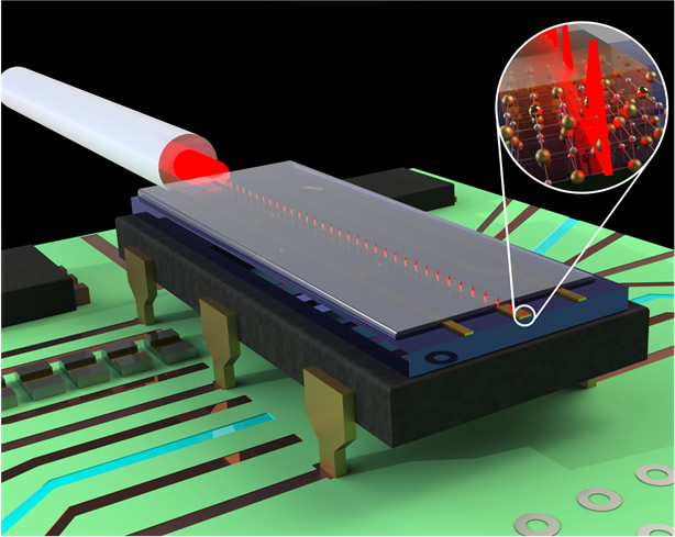
Mapping the nanoscale energy distributions of plasmonic hot-carriers
Contacts:
Harsha Reddy,
Zhaxylyk Kudyshev
Collaborators: Profs.
Pramod Reddy and
Edgar Meyhofer (University of Michigan, Ann Arbor)
Advisors: Profs. Vladimir Shalaev, Alexandra Boltasseva, and Alexander Kildishev
The generation of hot-carriers in plasmonic nanostructures, via plasmon decay, is of great current interest as hot-carriers play key roles in applications like photocatalysis, energy harvesting and in novel photodetection schemes that circumvent band-gap limitations. However, experimental quantification of steady-state energy distributions of hot-carriers in plasmonic nanostructures, which is critical for systematic progress, has not been possible. To address this outstanding challenge, we recently developed an experimental approach that enabled the direct measurement of hot-carrier energy distributions under steady-state conditions [1]. Specifically, we combined scanning probe-based quantum transport measurement techniques that record charge transport through single molecular junctions with nanoplasmonic experimental methods to directly quantify hot-carrier energy distributions in a key model system—a thin gold film that supports propagating surface plasmon polaritons. Furthermore, from our measurements, we obtained key physical insights on the role of Landau damping in producing hot-carriers and the contributions of different plasmonic modes towards hot-carrier generation. These studies were done in collaboration with Prof. Pramod Reddy and Prof. Edgar Meyhofer’s group at the University of Michigan, Ann Arbor.

On the left, graphic representation of the experimental approach to determine the energy distributions of plasmonic hot-carriers in a thin gold film. Surface plasmon polaritons are excited by illuminating the grating coupler with a laser, which leads to the generation of hot-carriers. The energy distributions of the generated hot-carriers are measured from the current flowing through a (voltage controlled) tunable molecular filter that selectively allows transport of carriers in a narrow energy window.
References:
[1] H. Reddy, K. Wang, Z. Kudyshev, L. Zhu, S. Yan, A. Vezzoli, S. J. Higgins, V. Gavini, A. Boltasseva, P. Reddy, V. M. Shalaev, and E. Meyhofer, "Determining plasmonic hot-carrier energy distributions via single molecule transport measurements,” Science, 10.1126/science.abb3457, 2020.
Quantum Nano-optics
Primary Contacts: Dr. Demid Sychev, Dr. Alexander Senichev
Secondary Contacts: Dr. Zhaxylyk Kudyshev, Xiaohui Xu, Zach Martin, Dr. Alexei Lagoutchev (Purdue)
Collaborators: Prof. Simeon Bogdanov, Prof. Alexey V. Akimov, Prof. Igor Aharonovitch, Prof. Jacob Khurgin, Prof. Sergey I. Bozhevolnyi, Prof. Ilya A. Rodionov
Advisors: Profs. Vladimir Shalaev, Alexandra Boltasseva, and Alexander Kildishev
Short project description:
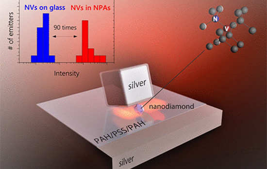
Color centers in diamond are crystalline defects that share many quantum properties with single atoms. At the same time, they are easier to manipulate than the latter and can be integrated into various solid-state devices. They are also promising platforms for realizing quantum devices such as nanoscale sensors, single-photon sources or quantum memories. Our research aims at discovering whether it is possible to draw on the potential of the dynamic field of nanophotonics in order to enhance or better harness the quantum properties of such systems. In particular, novel nanophotonic structures such as hyperbolic metamaterials, plasmonic waveguides, and plasmonic nanocavities are good candidates for increasing color centers’ spontaneous emission rate and controlling the directionality of their emission over a broad frequency range. The use of CMOS-compatible epitaxially grown plasmonic materials in the design of plasmonic structures promises a new level of functionality for a variety of integrated room-temperature quantum devices based on diamond color centers.
In the scope of this project, we have examined different types of nanodiamonds and identified the characteristics that lead to optimal optical and chemical properties. We have demonstrated broadband enhancement of emission from nitrogen-vacancy (NV) centers in nanodiamonds for both single NV centers and ensembles of NV centers using hyperbolic metamaterials (HMM), nanopatch antennas (NPA), and integrated plasmonic launchers (PL). As part of this work, we have studied the correlations between Purcell factor and optical measurements of NV’s spin state and the possibility to perform nanoscale sensing of photonic density of states using NV’s spin properties. By reducing the fluorescence lifetime from single NV centers, we also hope to enhance their single-photon emission rate such that we can perform a single-shot measurement of an NV center’s spin state. At the same time, we are also interested in developing nanoscale quantum devices from silicon-vacancy (SiV), germanium-vacancy (GeV), and lead-vacancy (PbV) centers in nanodiamonds. By enhancing the rate of emission from these defects, it may be possible to produce indistinguishable photons at room temperature. Similarly, we are also interested in developing quantum emitters in new materials such as 2D perovskite nanocrystals, transition metal dichalcogenide (TMDC) bilayers, and hexagonal boron nitride (hBN) flakes. Finally, we collaborate with other research groups to use defect centers in nanodiamonds and other materials for quantum sensing applications.
Papers Published:
- M. Y. Shalaginov, G. V. Naik, S. Ishii, M. N. Slipchenko, A. Boltasseva, J.-X. Cheng, A. N. Smolyaninov, E. Kochman, and V. M. Shalaev. "Characterization of nanodiamonds for metamaterial applications," Appl.Phys.B 105, 2, 191-195 (2011)
- M. Y. Shalaginov, S Ishii, J Liu, A Kildishev, VM Shalaev, "Broadband enhancement of spontaneous emission from nitrogen-vacancy centers in nanodiamonds by hyperbolic metamaterials" in 2013 Conference on Lasers and Electro-Optics (CLEO) and Quantum Electronics and Laser Science Conference (QELS), San Jose, CA, USA, 2013
- M. Y. Shalaginov, S.Ishii, J. Liu, J. Liu, J. Irudayaraj, A. Lagutchev, A.V. Kildishev, and V. M. Shalaev, "Broadband enhancement of spontaneous emission from nitrogen-vacancy centers in nanodiamonds by hyperbolic metamaterials", Appl. Phys. Lett. 102, 173114 (2013)
- M. Y. Shalaginov, V. V. Vorobyov, J. Liu, Marcello Ferrera, A. V. Akimov, A. Lagutchev, A. N. Smolyaninov, V. V. Klimov, J. Irudayaraj, A. V. Kildishev, A. Boltasseva and V. M. Shalaev, "Single-photon source based on NV center in nanodiamond coupled to TiN-based hyperbolic metamaterial" in 2014 Conference on Lasers and Electro-Optics (CLEO) and Quantum Electronics and Laser Science Conference (QELS), San Jose, CA, USA, 2014
- M. Y. Shalaginov, V. V. Vorobyov, J. Liu, M. Ferrera, A. V. Akimov, A. Lagutchev, A. N. Smolyaninov, V. V. Klimov, J. Irudayaraj, A. V. Kildishev, A. Boltasseva, and V. M. Shalaev, "Enhancement of single-photon emission from nitrogen-vacancy centers with TiN/(Al,Sc)N hyperbolic metamaterials", Laser Photonics Rev., 9, 1, 120-127 (2015) (*Cover Article*)
- M. Y. Shalaginov, A. Lagutchev, V. M. Shalaev, and A. V. Kildishev, "Effect of a hyperbolic metamaterial on radiation patterns of a single-photon source", in 2015 Conference on Lasers and Electro-Optics (CLEO) and Quantum Electronics and Laser Science Conference (QELS), San Jose, CA, USA, 2015
- S. Bogdanov, M. Y. Shalaginov, A. Akimov, P. Kapitanova, J. Liu, D. Woods, M. Ferrera, A. S. Laguchev, P Belov, J. Irudayaraj, A. Boltasseva, and V. M. Shalaev, "Engineering the spin-flip induced fluorescence contrast of diamond nitrogen
- O. A. Makarova, M. Y. Shalaginov, S. Bogdanov, A. V. Kildishev, A. Boltasseva, and V. M. Shalaev, Patterned multilayer metamaterial for fast and efficient photon collection from dipolar emitters, Optics Letters, Vol. 42, Issue 19, pp. 3968-3971 (2017)
- S. Bogdanov, M. Y. Shalaginov, A. Boltasseva, and V. M. Shalaev, Material platforms for integrated quantum photonics, Opt. Mater. Express 7, 111-132 (2017)
- S. Bogdanov, M. Y. Shalaginov, A. Akimov, A. S. Lagutchev, P. Kapitanova, J. Liu, D. Woods, M. Ferrera, P. Belov, J. Irudayaraj, A. Boltasseva, and V. M. Shalaev, Electron spin contrast of Purcell-enhanced nitrogen-vacancy ensembles in nanodiamonds, Phys. Rev. B 96, 035146 (2017)
- Simeon I. Bogdanov, Mikhail Y. Shalaginov, Alexei S. Lagutchev, Chin-Cheng Chiang, Deesha Shah, Alexandr S. Baburin, Ilya A. Ryzhikov, Ilya A. Rodionov, Alexander V. Kildishev, Alexandra Boltasseva, and Vladimir M. Shalaev, Ultrabright Room-Temperature Sub-Nanosecond Emission from Single Nitrogen-Vacancy Centers Coupled to Nanopatch Antennas, Nano Letters (2018)
- S.I. Bogdanov, A. Boltasseva, and V.M. Shalaev, Overcoming quantum decoherence with plasmonics, Science, v. 364, pp. 532-533 (2019)
- S. I. Bogdanov, O. A. Makarova, X. Xu, Z. O. Martin, A. S. Lagutchev, M. Olinde, D. Shah, S. N. Chowdhury, A. R. Gabidullin, I. A. Ryzhikov, I. A. Rodionov, A. V. Kildishev, S. I. Bozhevolnyi, A. Boltasseva, V. M. Shalaev, and J. B. Khurgin, Ultrafast quantum photonics enabled by coupling plasmonic nanocavities to strongly radiative antennas, Optica v. 7, pp. 463-469 (2020)
MURI: Near-Field Radiative Heat Transfer between Nanostructured Materials
Primary Contacts:
Zelong "Bruce" Ding,
Harsha Reddy,
Zhaxylyk Kudyshev
Advisors: Profs.
Vladimir Shalaev and
Alexandra Boltasseva
Collaborators: Profs. Pramod Reddy (UMich), Edgar Meyhofer (UMich), and Shanhui Fan (Stanford)
Short project description:
NFRHT between two nanostructured metasurfaces separated by a nano gap
The principles of near-field (NF) radiative heat transfer (RHT), i.e. the transfer of heat or energy across nanoscale gaps via electromagnetic fields, are of great interest as several remarkable phenomena arise exclusively in the NF. Far-field (FF) RHT, explored at the beginning of the 20th century, culminated in Max Planck’s theory of RHT and played a central role in the development of quantum mechanics. However, Planck explicitly noted that his FFRHT theory was only applicable to scenarios where the separation between the hot and cold objects is significantly larger than the Wien’s wavelength (~10 μm at room temperature). With the advent of micro- and nanotechnology that features nanoscale dimensions, an urgent need to understand thermal radiation in nanoscale gaps has emerged.
Recent experiments have measured RHT rates in the NF [1-3], which have revealed several orders of magnitude enhancements in RHT rates, compared to FFRHT, when the separation between the hot and cold objects is reduced to length scales below Wein’s wavelength. Specifically, close to 1,000 fold enhancements in RHT were observed from experiments for gap sizes below 100 nm [3, 4]. These exciting discoveries have spurred researchers to explore ways to further engineer and enhance NFRHT. In this regard, recent theoretical studies [5-7] have predicted the possibility of further enhancing NFRHT via spectral engineering with metasurfaces that feature judiciously patterned nanostructures. Our group is currently working towards testing the validity of these interesting theoretical predictions. We are closely working with our collaborators (Prof. Shanhui Fan, Prof. Pramod Reddy and Prof. Edgar Meyhofer) towards fabricating these metasurfaces on suspended picowatt resolution calorimeters (designed and fabricated in Prof. Pramod Reddy and Prof. Edgar Meyhofer’s group). The performance of the fabricated metasurfaces will be characterized by our collaborators at University of Michigan, Ann Arbor, using their state-of-the-art nanopositioning platform. Along with their fundamental importance, these studies are expected to play a crucial role in the development of innovative thermal technologies, ranging from thermophotovoltaics to near-field photonic refrigeration.
References:
[1] Rousseau, E. et al. Radiative heat transfer at the nanoscale. Nat. Photonics. 3, 514-517 (2009).
[2] Shen, S. et al. Surface phonon polaritons mediated energy transfer between nanoscale gaps. Nano Lett. 9, 2909-2913 (2009).
[3] Kim, K. et al. Radiative heat transfer in the extreme near-field. Nature 528, 387-391 (2015).
[4] Song, B. et al. Radiative heat conductances between dielectric and metallic parallel plates with nanoscale gaps. Nat. Nanotechnol. 11, 509-514 (2016).
[5] Fernandez-Hurtado, V. et al. Enhancing Near-Field Radiative Heat Transfer with Si-Based Metasurfaces. Phys. Rev. Lett. 118, 203901 (2017).
[6] Miller, O.D. et al. Limits to the Optical Response of Graphene and Two-Dimensional Materials. Nano Letters 17, 5408-5415 (2017).
[7] Miller, O.D. et al. Shape-Independent Limits to Near-Field Radiative Heat Transfer. Phys. Rev. Lett. 115, 204302 (2015).
Robust Vivid Plasmonic Color Printing
Primary Contact: Sarah Nahar Chowdhury
SAdditional Contacts: Dr. Alexei S. Lagoutchev, Zhaxylyk Kudyshev
Collaborators: Dr. Piotr Nyga, Dr. Esteban Garcia
Advisors: Profs. Vladimir Shalaev, Alexandra Boltasseva, Alexander Kildishev
Short project description:
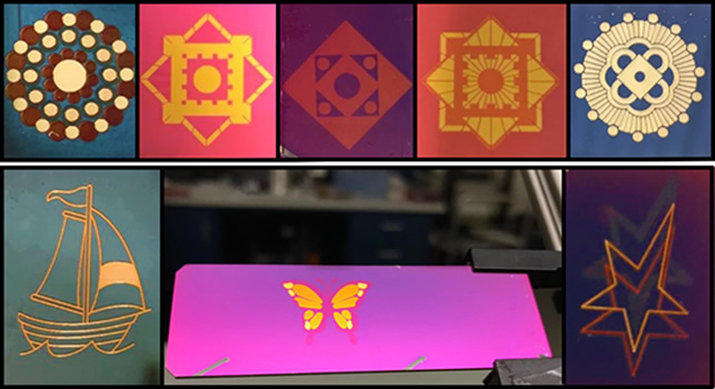
We demonstrate a method of generation of bright colors through laser post processing on a multilayer structure comprising of a very thin layer of Ag semicontinuous metal film (SMF) on a dielectric spacer with mirror. Such a structure is not only inexpensive, environment-friendly, and non-bleaching but also has the potential of microscopic printing to 1.44µm (approx.). The process employs a SMF comprising of random nanostructures with different particle sizes and shapes which are responsible for absorption at different wavelengths. SMF on spacer with mirror (SMFM) upon interaction with light can localize electromagnetic energy in nanoscale regions. With laser illumination, reshaping and fragmentation of metallic nanostructures occur in the vicinity of these regions and change in optical response occurs. Through varying the scan speed, number of pulses, energy density, power, and exposure time of 800 nm, 80 fs, 1 kHz laser illuminated on the structure, highly contrasting and vivid colors can be obtained. This structure can be fabricated easily and can be applied to the macroscopic, mesoscopic and nanoscopic printing of innovatory fade-free artistic images as one example of application.
Papers Published:
[1] Laser-induced color printing on semicontinuous silver films: red, green and blue, Piotr Nyga, Sarah N Chowdhury, Zhaxylyk Kudyshev, Mark D Thoreson, Alexander V Kildishev, Vladimir M Shalaev, Alexandra Boltasseva, Optical Materials Express 9 (3), 1528-1538
[2] Laser Color Printing on Semicontinuous Silver Films, Sarah N Chowdhury, Piotr Nyga, Zhaxylyk Kudyshev, Alexander V Kildishev, Vladimir M Shalaev, Alexandra Boltasseva, CLEO: Science and Innovations, JW2A. 55
[3] Laser Color Printing on Semicontinuous Ag Films, Sarah N. Chowdhury, Piotr Nyga, Zhaxylyk Kudyshev, Alexander V. Kildishev, Vladimir M. Shalaev, Alexandra Boltasseva, Women in Engineering Program 50th Anniversary Celebration
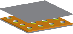
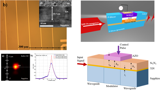
Transdimensional Plasmonic Materials
Primary Contact: Deesha Shah
Collaborators: Prof. Igor Bondarev (North Carolina Central University), Dr. Arrigo Calzolari (CNR-Nano, Italy)
Advisors: Profs. Vladimir Shalaev and Alexandra Boltasseva
Short project description:
![]()
As plasmonic materials transition from the three dimensional (3D) form to two dimensional (2D), unique optical and electronic phenomena arise that are unattainable in bulk materials and conventional thin films. Similar to 2D materials, ultra-thin films in the transdimensional regime spanning a few atomic layers, known as transdimensional materials (TDMs), are expected to exhibit strong dependences on structural and compositional properties, as well as extreme sensitivities to external optical and electrical perturbations. Additionally, the small thicknesses may lead to strongly confined surface plasmons and unique quantum phenomena such as forbidden atomic transitions and enhanced nonlinearities. The strong tunability and light confinement offered by TDMs has resulted in a search for atomically thin material platforms that facilitate active metasurfaces with novel functionalities in the visible and NIR range.
Epitaxial thin films are particularly ideal in investigating the size dependent response as there are no contributions to losses from grain boundaries. Epitaxial TiN can be routinely grown on substrates such as c-sapphire and MgO with standard sputtering processes, enabling the formation of continuous ultrathin films down to 1 nm (5 monolayers) while maintaining high quality. Due to its high-quality growth, chemical stability, and tailorable optical properties, TiN is an ideal material choice to study plasmonic properties at the atomic level. We are investigating the thickness dependent properties of ultra-thin TiN experimentally and theoretically, which hold great promise for realizing a new generation of tunable metasurfaces with quantum and nonlocal effects.
Papers:
[1] Shah, D., Kudyshev, Z. A., Saha, S., Shalaev, V. M. & Boltasseva, A. Transdimensional material platforms for tunable metasurface design. MRS Bull. 45, 188–195 (2020).
[2] Boltasseva, A. & Shalaev, V. M. Transdimensional Photonics. ACS Photonics 6, 1–3 (2019).
[3] Shah, D. et al. Controlling the Plasmonic Properties of Ultrathin TiN Films at the Atomic Level. ACS Photonics 5, 2816–2824 (2018).
[4] Bondarev, I. V., Mousavi, H. & Shalaev, V. M. Optical response of finite-thickness ultrathin plasmonic films. MRS Commun. 8, 1092–1097 (2018).
[5] Bondarev, I. V. & Shalaev, V. M. Universal features of the optical properties of ultrathin plasmonic films. Opt. Mater. Express 7, 3731–3740 (2017).
[6] Shah, D., Reddy, H., Kinsey, N., Shalaev, V. M. & Boltasseva, A. Optical Properties of Plasmonic Ultrathin TiN Films. Adv. Opt. Mater. 5, 1700065 (2017).
Refractory Plasmonics
Primary Contact: Bruce Ding
Additional Contact: Harshavardhanareddy Eragamreddy
Advisors: Prof. Vladimir M. Shalaev, Prof. Alexandra Boltasseva, Prof. Alexander Kildishev
Collaborators: Prof. Ernesto Marinero, Prof. Peter Bermel, Prof. Tim Sands, Prof. Ali Shakouri, Prof. Ted Norris, Prof. Oana Malis, Prof. Sergey Bozhevolnyi
Short project description:
Some of the proposed plasmonic applications require extreme operating conditions such as high temperatures and chemically aggressive environment. Conventional plasmonic materials such as noble metals bring limitations due to their lower melting point, softness etc. Refractory materials, exhibiting high melting points and chemical stability above 2000 oC, with plasmonic properties in the visible and near infrared regions can be the solutions to major problems hindering the improvement of potentially high-impact applications such as heat assisted magnetic recording (HAMR), solar/thermophotovoltaics (S/TPV) and solar thermoelectric generators (STEG).
Transition metal nitrides, in particular titanium nitride (TiN) and zirconium nitride (ZrN), are known as refractory materials and exhibit plasmonic resonances in the visible and near infrared regions. Nanoantennas made of refractory plasmonic materials can be employed as durable near field transducers for HAMR heads where antenna temperatures are estimated to be above 400°C. Furthermore, ultrathin broadband absorbers and selective emitters made of refractory plasmonic materials offer durability at higher temperatures and higher overall device efficiencies for S/TPVs and STEGs.
Papers:
- J. Liu, U. Guler, A. Lagoutchev, A. Kildishev, O. Malis, A. Boltasseva, V. M. Shalaev, "Quasi-coherent thermal emitter based on refractory plasmonic materials", Opt. Mater. Express, v. 5, pp. 2721-2728 (2015)
- U. Guler, S. Suslov, A. V. Kildishev, A. Boltasseva, V. M. Shalaev, "Colloidal plasmonic titanium nitride nanoparticles: Properties and applications", Nanophotonics, DOI: 10.1515/nanoph-2015-0017 (*Invited Research Paper*)
- U. Guler, A. Boltasseva, V. M. Shalaev, "Plasmonics on the slope of enlightenment: the role of transition metal nitrides", Faraday Discuss. 178, 71-86 (2015) (*Invited Research Paper*)
- U. Guler, V. M. Shalaev, and A. Boltasseva, "Nanoparticle Plasmonics: Going Practical with Transition Metal Nitrides," Materials Today, 18, 227-237 (2015) (*Invited Review Paper*)
- W. Li, U. Guler, N. Kinsey, G. V. Naik, A. Boltasseva, J. Guan, V. M. Shalaev, and A. V. Kildishev, "Refractory Plasmonics with Titanium Nitride: Broadband Metamaterial Absorber," Adv. Mater. 26, 7959-7965 (2014). (*Cover Article*)
- U. Guler, A. Boltasseva, and V. M. Shalaev, Refractory Plasmonics, Science 344, 263-264 (2014)
- U. Guler, J. C. Ndukaife, G. V. Naik, A. G. A. Nnanna, A. V. Kildishev, V. M. Shalaev, and A. Boltasseva, Local Heating with Lithographically Fabricated Plasmonic Titanium Nitride Nanoparticles, Nano Letters 13, 6078-6083 (2013)
- U. Guler, G. V. Naik, A. Boltasseva, V. M. Shalaev, and A. V. Kildishev, Performance Analysis of Nitride Alternative Plasmonic Materials for Localized Surface Plasmon Applications, Appl. Phys. B 107, 285-291 (2012)
- Urcan Guler, Wei Li, Alexandra Boltasseva, Alexander Kildishev, Vladimir M. Shalaev, "Titanium Nitride as a Refractory Plasmonic Material for High Temperature Applications," in CLEO: 2014
- Jingjing Liu, Urcan Guler, Wei Li, Alexander V. Kildishev, Alexandra Boltasseva, and Vladimir M. Shalaev, "High-temperature plasmonic thermal emitter for thermo-photovoltaics," in CLEO: 2014
- U. Guler, W. Li, N. Kinsey, G. V. Naik, A. Boltasseva, J. Guan, A. V. Kildishev, and V. M. Shalaev, Plasmonic Titanium Nitride Nanostructures for Perfect Absorbers, in Renewable Energy and the Environment, OSA Technical Digest (online) (Optical Society of America, 2013), PW3B.8
- U. Guler, G. Naik, A. Boltasseva, V. Shalaev, and A. Kildishev, Nitrides as alternative materials for localized surface plasmon applications, in Frontiers in Optics 2012/Laser Science XXVIII, OSA Technical Digest (online) (Optical Society of America, 2012), FTh4A.2
- K. Chaudhuri, U. Guler, S. Azzam, H. Reddy, S. Saha, E. Marinero, A. V. Kildishev, V. M Shalaev, A. Boltasseva, Remote Sensing of High Temperatures with Refractory, Direct-Contact Optical Metacavity, ACS Photonics (2020)
- K. Chaudhuri, U. Guler, S. Azzam, H. Reddy, S. Saha, E. Marinero, A. V. Kildishev, V. M. Shalaev, A. Boltasseva, Remote Sensing of High Temperatures with Refractory, Direct-Contact Optical Metacavity, ACS Photonics, v. 7, pp. 472–479 (2020)
Novel Optics with Metasurfaces
Primary Contact: Soham Saha
Additional Contact: Deesha Shah, Sarah Nahar Chowdhury
Advisors: Prof. Vladimir Shalaev, Prof. Alexandra Boltasseva, Prof. Alexander Kildishev
Collaborator: Dr. Amr Shaltout
Short project description:
Subwavelength cavities are obtained by replacing conventional mirrors with reflecting metasurfaces that introduce arbitrary phase-shifts compensating for reduced accumulated phase through the ultra-small cavity. Same concept works for waveguides, where propagating modes require round trip phase-shift in the transverse direction to be integer multiple of 2p. This causes the minimum cross-section size to be the diffraction limit of ?/2, and introducing reflecting metasurfaces change the phase condition allowing the cross-section to go below the diffraction limit.
We design, fabricate, and experimentally demonstrate optically active metasurfaces of ?/50 thickness. Our approach is built on supercell metasurface design methodology: by judiciously designing the location and orientation of individual antennas in the structural supercells, we achieve effective chiral metasurfaces through a collective operation of non-chiral antennas.
Ultrathin metamaterial layers are modeled by a homogeneous bi-anisotropic film to model various kinds of broken symmetries in photonic nanostructures. It successfully modeled rotational asymmetry, mirror asymmetry and directional asymmetry. It has been also used to replace an array of nanostructured plasmonic elements (e.g. V-shape antennas) with a thin metasurface of equivalent bianisotropic tiles, which enabled significant reduction of computational load for simulation purposes.
Papers Published:
- A. M. Shaltout, A. V. Kildishev, and V. M. Shalaev "Ultra-Small Cavity with Reflecting Metasurfaces", US patent application
- A. M. Shaltout, A. V. Kildishev, V. M. Shalaev, "Compact Subwavelength Cavities Using Reflecting Metasurfaces," Accepted for 2014 Conference on Lasers and Electro-Optics (CLEO) and Quantum Electronics and Laser Science Conference (QELS), San Jose, CA, USA, 2014
- A. M. Shaltout, V. M. Shalaev, and A. V. Kildishev "Waveguides with Hyperbolic Metasurface Claddings", ACES 2014 Conference, Jacksonsville, Fl, USA, 2014. (4th place winner of student paper competition)
- P.R. West, J. L. Stewart, A. Kildishev, V.M. Shalaev, V. Shkunov, F. Strohkendl, Y. Zakharenkov, R. Dodds, R. Byren, "All-dielectric subwavelength metasurface focusing lens," submitted to Optics Express, 2014
- A. M. Shaltout, J. Liu, V. M. Shalaev, and A. V. Kildishev, "Optically Active Metasurfaces with Nonchiral Plasmonic Nano-antennas" submitted for journal publication
- A. M. Shaltout, J. Liu, A. V. Kildishev, and V. M. Shalaev, Broadband Optical Chirality Using Ultrathin Metasurface, in 2013 Conference on Lasers and Electro-Optics (CLEO) and Quantum Electronics and Laser Science Conference (QELS), San Jose, CA, USA, 2013
- F. Ding, N. Kinsey, J. J. Liu, Z. X. Wang; V. M. Shalaev and A. V. Kildishev, "Unidirectional Surface Plasmon Polariton Coupler in the Visible Using Metasurfaces," Accepted for 2014 Conference on Lasers and Electro-Optics (CLEO) and Quantum Electronics and Laser Science Conference (QELS), San Jose, CA, USA, 2014
- J. Liu, A. M. Shaltout, X. Ni, V. M. Shalaev, and A. V. Kildishev, "Approximating metasurfaces with bianisotropic tiles" ACES 2014 Conference (Invited paper), Jacksonsville, Fl, USA, 2014
- J. Liu, A. M. Shaltout, X. Ni, V. M. Shalaev, A. V. Kildishev, Experimental validation of a new bianisotropic parameter retrieval technique using plasmonic metasurfaces made of V-shape antennas, in The SPIE Optics+Photonics 2013 Advance, San Diego, CA, USA, 2013
- A. M. Shaltout, V. M. Shalaev, A. V. Kildishev, Homogenization of bi-anisotropic metasurfaces, Optics Express, Vol 21, Issue 19, pp. 21941 - 21950 (2013)
- A. M. Shaltout, V. M. Shalaev, A. V. Kildishev, "Bi-Anisotropic Homogenization of Metasurfaces," ACES 2013 Conference, Monterey, CA, USA, 2013
- A.M. Shaltout, V.M. Shalaev, M.L. Brongersma, Spatiotemporal light control with active metasurfaces, Science 364, eaat3100 (2019). DOI: 10.1126/science.aat3100
- A. M. Shaltout , K. G. Lagoudakis, J. van de Groep, S. J. Kim, J. Vučković, V. M. Shalaev, M. L. Brongersma, Spatiotemporal light control with frequency-gradient metasurfaces, Science, v. 365, pp. 374-377 (2019); DOI: 10.1126/science.aax2357
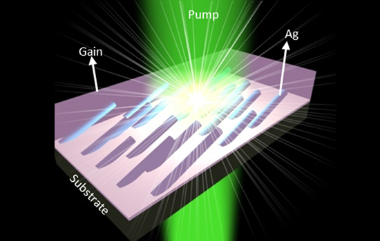
Nanolasers
Primary Contact: Dr. Xiangeng Meng
Additional Contact: Dr. Alexei S. Lagoutchev
Advisors: Prof. Vladimir Shalaev, Prof. Alexandra Boltasseva, Prof. Alexander Kildishev
Short project description:
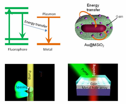
The nanolaser project aims to develop compact light sources using plasmonic nanostructures as resonant cavities. The nanolaser is based on amplification of surface plasmons ? surface waves propagating along a metallic-dielectric interface, thus also entitled spaser (short for surface plasmon amplification by stimulated emission of radiation). The fact that plasmon modes have no cutoff allows for creation of compact light sources at real nanometer scale in terms of either the device size or optical mode volume. There are currently several challenges that are being addressed in this area, including the control of spasing propagation direction and the achievement of spasing in the visible. Numerical simulations are being conducted to help understanding of spasing dynamics.
Papers Published:
- X. Meng, U. Guler, A. V. Kildishev, K. Fujita, K. Tanaka, and V. M. Shalaev, "Unidirectional Spaser in Symmetry-Broken Core-Shell Nanocavity", Sci. Rep. 3, 1241 (2013)
- X. Meng, A. V. Kildishev, K. Fujita, K. Tanaka, and V. M. Shalaev, "Wavelength-Tunable Spasing in the Visible", Nano Lett. 13, 4106-4112 (2013)
- X. Meng, J. Liu, A. V. Kildishev, and V. M. Shalaev, "Highly Directional Spaser Array for the Red Wavelength Region", Laser Photonics Rev. 8, 896-903 (2014)
- J. Fang; L. Prokopeva; J. Trieschmann; N. Arnold; A. V. Kildishev, "PhotonicsGAIN-0D," DOI: 10.4231/D3PK07200, (2013)
- S. Azzam et al, Dynamically Controlled Random Lasing with Colloidal Titanium Carbide MXene. OMEX (2020)
- S. I. Azzam, J. Fang, J. Liu, Z. Wang, N. Arnold, T. A. Klar, L. J. Prokopeva, X. Meng, V. M. Shalaev, A. V. Kildishev, Exploring Time‐Resolved Multiphysics of Active Plasmonic Systems with Experiment‐Based Gain Models, Laser & Photonics Reviews, v. 13, no. 1 (2019): 1800071
- S. I. Azzam, A. V. Kildishev, R. M. Ma, C. Z. Ning, R. Oulton, V. M. Shalaev, M. I. Stockman, J. L. Xu, and X. Zhang, Ten years of spasers and plasmonic nanolasers, Light: Science & Applications, v. 9, no. 1, pp. 1-21 (2020)
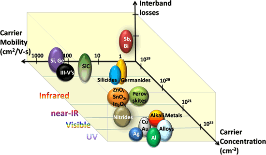
Alternative Plasmonic Materials
Primary Contacts: Nate Kinsey, Jongbum Kim
Additional Contacts: Aveek Dutta, Zhouxian Wang, Sajid Choudhury
Advisor: Prof. Alexandra Boltasseva
Collaborator: Prof. Vladimir Shalaev
Short project description:
Plasmonics is a research area merging the fields of optics and nanoelectronics by confining light with relatively large free-space wavelength to the nanometer scale - thereby enabling a family of novel devices. Current plasmonic devices at telecommunication and optical frequencies face significant challenges due to losses encountered in the constituent plasmonic materials. These large losses seriously limit the practicality of these metals for many novel applications. We are now in the process of finding materials with improved optical performance, as well as applying these new materials to novel devices. These materials include transparent conductive oxides (TCOs) such as indium tin oxide (ITO), gallium zinc oxide (GZO), and aluminum zinc oxide (AZO) and metallic nitrides such as titanium nitride (TiN), zirconium nitride (ZrN), hafnium nitride (HfN). TCOs have been shown to be effective plasmonic materials in the infrared region while transition metal nitrides extend into the visible spectrum. These materials are currently being used by the Boltasseva Group in novel plasmonic applications such as integrated plasmonic devices, tunable plasmonics, and particle trapping.
Selected Papers
- G. V. Naik, V. M. Shalaev, A. Boltasseva, Alternative Plasmonic Materials: beyond gold and silver, Advanced Materials, vol. 25, no. 24, pp. 3264-3294, 2013. (*Inside Cover picture, highlighted by Purdue News*)
- G. V. Naik, J. L. Schroeder, X. Ni, A. V. Kildishev, T. D. Sands, A. Boltasseva, "Titanium nitride as a plasmonic material for visible and near-infrared wavelengths," Optical Materials Express 2 (4), 478-489 (April 1 2012) (*Top OSA download in April 2012, highlighted in OSA press release and key industry media outlets Science Daily, NSF Science 360, Red Orbit, Photonics.com, April 2012*)
- J. B. Khurgin and A. Boltasseva, Reflecting upon the losses in plasmonics and metamaterials, MRS Bulletin, vol. 37, no. 8, pp. 768-779, 2012. (*Invited*)
- A. Boltasseva and H. Atwater, Low-loss plasmonic metamaterials, Science Perspective, Science, vol. 331, pp. 290-291, 2011. (*Featured in Nature photonics 5, 139-140, 2011 and number of scientific and technological websites*)
- G. V. Naik, J. Kim, A. Boltasseva, Oxides and nitrides as alternative plasmonic materials in the optical range, Optical Materials Express, vol. 1, no. 6, pp. 1090-1099, 2011. (*Invited*) (*Top downloaded until 2013, Highlighted in OSA News Release, September 22, 2011*)
- P. R. West, S. Ishii, G. V. Naik, N. K. Emani, V. M. Shalaev, A. Boltasseva, Searching for better plasmonic materials, Laser & Photonics Reviews, vol. 4, no. 6, pp. 795-808, 2010. (*Cover picture, highlighted by Purdue News*)
- G. V. Naik, B. Saha, J. Liu, S. M. Saber, E. Stach, J. MK Irudayaraj, T. D. Sands, V. M. Shalaev, A. Boltasseva, "Epitaxial superlattices with titanium nitride as a plasmonic component for optical hyperbolic metamaterials," submitted to PNAS (2013)
- B. Saha, G. Naik, V. P. Drachev, A. Boltasseva, E. E. Marinero, T. D. Sands, "Electronic and optical properties of ScN and (Sc,Mn)N thin films deposited by reactive DC-magnetron sputtering", Journal of Applied Physics 114 (6), 063519, DOI: 10.1063/1.4817715 (August 14 2013
- G. V. Naik, J. Liu, A. V. Kildishev, V. M. Shalaev, A. Boltasseva, "Demonstration of Al:ZnO as a plasmonic component of near-infrared metamaterials," Proceedings of the National Academy of Sciences 109 (23), 8834-8838 DOI: 10.1073/pnas.1121517109 (June 5 2012
Plasmonics with Graphene & Beyond
Primary Contact: Krishnakali Chaudhuri, Di Wang
Advisors: Profs. Alexandra Boltasseva, Alexander Kildishev, Vladimir Shalaev
Collaborators: Prof. Joerg Appenzeller, Prof. Zhihong Chen
Short project description:
This project falls under the umbrella of research program carried out at the recently established Purdue Quantum Center.
Short project description:
Plasmonics offers an exciting route to sub-wavelength optoelectronics by confining the optical fields below the diffraction limit. This is achieved by employing metal nanostructures resonant at a particular optical wavelength. Dynamic control of these plasmonic resonances at optical wavelengths is critical for many applications like integrated modulators and switches. In our group we have explored some of these exciting possibilities that result from real-time tuning of plasmonic resonances using graphene.
Graphene - a perfect 2D material consisting of single monolayer of carbon atoms, has some fascinating electrical and optical properties. We exploited the highly tunable interband transitions in graphene to dynamically modulate the plasmonic resonance in bow-tie nanoantennas and Fano resonant plasmonic nanostructures. We have also developed an accurate time domain model for performing numerical simulations. Currently, we are working on a graphene photodetector with a hybrid plasmonic fractal metasurface design which improves the broadband operation as well as the responsivity.
Beyond graphene, we have also been interested in working with other two dimensional materials e.g. transition metal dichalcogenides (TMDs) such as MoS2, MoSe2, WSe2, WS2 etc. Amongst their many interesting properties, we would like to exploit the strong signature of room temperature excitons and make hybrid plasmon-excitonic systems to manipulate & enhance the photo detection or even the PL efficiency of the emitters. We also have efforts towards measuring the optical properties of different two dimensional materials through the broad optical range of VIS through MIR and their electrical tunability, eventually integrating them into devices with new plasmonic materials such as nitrides and TCOs. We have some recent efforts towards finding new 2D materials plasmonic in MIR as well.
Papers Published:
- Naresh K. Emani, Ting-Fung Chung, Alexander V. Kildishev, Vladimir M. Shalaev, Yong P. Chen, Alexandra Boltasseva, "Electrical modulation of Fano resonance in plasmonic nanostructures using Graphene", Nano Letters 14 78 (2014).
- Naresh K. Emani, T. F. Chung, X. Ni, A. V. Kildishev, Y. P. Chen, and A. Boltasseva, "Electrically Tunable Damping of Plasmonic Resonances with Graphene," Nano letters 12, 5202-5206 (2012).
- L. J. Prokopeva, N. K. Emani, A. Boltasseva, and A. Kildishev, "Time Domain Modeling of Tunable Response of Graphene," in CLEO: 2013, San Jose, California, 2013, p. QTh1A.8.
- N. K. Emani, T.-F. Chung, L. Prokopeva, A. Kildishev, Y. Chen, and A. Boltasseva, "Tuning Fano Resonances with Graphene," in CLEO: 2013, San Jose, California, 2013, p. CW3O.4.
Integrated Nanophotonic Devices with Alternative Materials
Primary Contact: Nate Kinsey
Additional Contact: Aveek Dutta
Advisors: Prof. Alexandra Boltasseva, Prof. Vladimir Shalaev
Collaborators: Prof. Sergey Bozhevolnyi, Prof. Marcello Ferrera
Short project description:
In order to continue the rapid increase the computation technologies, additional solutions should be investigated to supplement current microelectronic chips. One of the most promising technologies is light. Plasmonic devices, which couple light to the oscillations of free electrons at a metal-dielectric interface, provide several advantages over photonic solutions. Plasmonic devices can have reduced coupling loss to ultra-compact active devices (modulators, sensors, switches, etc.), have a large sensitivity to the metal-dielectric surface, and can carry both electrical and optical signals. Our research is focused on realizing high-performance devices such as low-loss waveguides, ultra-compact modulators, and sensors using a practical material platform (titanium nitride, doped zinc oxide, and supporting materials) that are compatible with standard semiconductor fabrication techniques. We collaborate with Dr. Sergey Bozhevolnyi from the University of Southern Denmark on this project.
- N. Kinsey, M. Ferrera, V.M. Shalaev, A. Boltasseva, "Examining nanophotonics for integrated hybrid systems: a review of plasmonic interconnects and modulators using traditional and alternative materials," JOSA B 32 (1), 121-142 (January 1, 2015) (*invited*)
- N. Kinsey, C. DeVault, J. Kim, M. Ferrera, V.M. Shalaev, and A. Boltasseva, "Epsilon-Near-Zero Al-Doped ZnO for Ultrafast Switching at Telecom Wavelengths," Optica, vol. 2, no. 7, 2015. (see supplementary materials)
- N. Kinsey, M. Ferrera, G.V. Naik, V.E. Babicheva, V.M. Shalaev, A. Boltasseva, "Experimental demonstration of titanium nitride plasmonic interconnects," Optics Express in Press, April 2014.
- V. Babicheva, N. Kinsey, G. Naik, M. Ferrera, A. Lavrinenko, V.M. Shalaev, and A. Boltasseva, "Towards CMOS-compatible nanophotonics: Ultra-compact modulators using alternative plasmonic materials," Optics Express, vol. 21, no. 22, 2013.
Completed projects
Optical Properties of Alternative Plasmonic Materials
Primary Contact: Nate Kinsey
Additional Contact: Clayton DeVault
Advisors: Profs. Alexandra Boltasseva and Vladimir Shalaev
Collaborators: Prof. Marcello Ferrera, Prof. Carl Bonner, Prof. Vladimir Gavrilenko, Prof. Alexander Kildishev, Prof. Eric Van Stryland, Prof. David Hagan
Short project description:
Alternative plasmonic materials provide an exceptional potential for application in numerous areas of nanophotonics. However, some of the more basic material properties are not well investigated. In this project we are studying both the linear and nonlinear optical properties of alternative plasmonic materials.
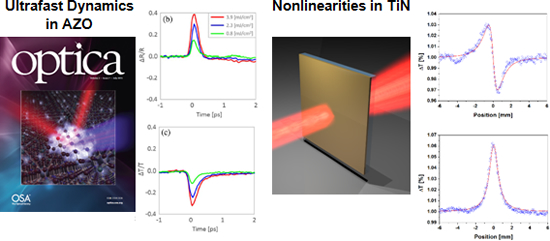
One aspect of this research has focused on the ultrafast carrier dynamics in aluminum doped zinc oxide (AZO). Here we pump the AZO above bandgap to excite excess free carriers which modifies the optical properties of the material until the excess carriers recombine. The probe the optical properties in the epsilon-near-zero regime which leads to an enhancement of the response. Ultrafast (<1 ps) dynamics with large change (~40% in reflection) are observed for thin films suggesting AZO may be useful for all-optical ultrafast sensing, communication, and spectroscopy. We collaborate with Prof. Marcello Ferrera (Heriot Watt University)
Another area of our study focuses on the nonlinear optical properties of alternative materials. The study of these materials is particularly important since the transition metal nitride family (titanium nitride, zirconium nitride, hafnium nitride, and tantalum nitride) can withstand significantly larger temperatures (i.e. optical intensities) than noble metal films which is critical for nonlinear applications. In addition, they are biocompatible and CMOS compatible. These properties make them ideal for applications in biological/medial sensing and integrated nonlinear optics applications. An example of this work is the study of effective third order nonlinear properties in TiN thin films using the z-scan technique where we compare the response with traditional metals. With a better understanding of the nonlinear properties of this family of materials, we hope to develop novel sensing and integrated nonlinear devices. We collaborate with Prof. Carl Bonner and Prof. Vladimir Gavrilenko (Norfolk State University) as well as Prof. Eric Van Stryland and Prof. David Hagan (University of Central Florida) on this project.
- N. Kinsey, C. DeVault, J. Kim, M. Ferrera, V.M. Shalaev, and A. Boltasseva, "Epsilon-Near-Zero Al-Doped ZnO for Ultrafast Switching at Telecom Wavelengths," Optica, vol. 2, no. 7, 2015.
- N. Kinsey et al, "Effective Third-Order Nonlinearities in Refractory Plasmonic TiN Thin Films," submitted to Optical Materials Express, 2015.
- J. Kim, G. V. Naik, N. K. Emani, U. Guler, A. Boltasseva, "Plasmonic Resonances in Nanostructured Transparent Conducting Oxide Films," IEEE Journal of Selected Topics in Quantum Electronics 19, 4601907, 2013 (*invited*)
- J. Kim, Y. Zhao, G. Naik, N. Emani, U. Guler, A. Kildishev, A. Alu, A. Boltasseva, ''Nanostructured Transparent Conductive Oxide Films for Plasmonic Applications,'' contribution QTh3B.8, CLEO/QELS 2013, San Jose, CA, USA, June 9-14, 2013
- J. Kim, B. Memarzadeh, A. Dutta, S. M. Choudhury, A. V. Kildishev, H. Mosallaei, and A. Boltasseva, "GZO/ZnO Multilayered nanodisk metasurface to engineer the plasma frequency" CLEO, 2014
- J. Kim, Y. Zhao, A. Dutta, S. M. Choudhury, A. V. Kildishev, A. Alu, and A. Boltasseva, "Nanostructured Transparent Conducting Oxide Films for Polarization Control with Plasmonic Metasurfaces" CLEO, 2014
- Justus C. Ndukaife, Avanish Mishra, Urcan Guler, A. G. Agwu Nnanna, Steven T. Wereley, Alexandra Boltasseva, "Photothermal Heating Enabled by Plasmonic Nanostructures for Electrokinetic Manipulation and Sorting of Particles", ACS Nano 8, no. 9 (2014): 9035-9043.
- Justus C. Ndukaife, Alexander V. Kildishev, A. G. Agwu Nnanna, Steven T. Wereley, Vladimir M. Shalaev, Alexandra Boltasseva, "Hybrid Electroplasmonic NanoTweezer (HENT): Highly resolved long-range optofluidic control and delivery of single particles on-demand" (under review).
- Justus C. Ndukaife, Alexander V. Kildishev, A. G. Agwu Nnanna, Steven T. Wereley, Vladimir M. Shalaev, Alexandra Boltasseva, "Electrothermoplasmonic Flow for Plasmon-assisted Optical Trapping", (invited talk for 2015 SPIE Conference on Plasmonics: Metallic Nanostructures and their Optical Properties XIII San Diego, California, USA, August 12, 2015) .
- Justus C. Ndukaife, A. G. Agwu Nnanna, Steven T. Wereley, Alexandra Boltasseva, "Harnessing Intrinsic Photo-induced Heating of Plasmonic Nanostructures for Manipulation of Micro and Nanoscale Objects", (accepted for oral presentation at ASME IMECE 2015 Conference, Houston Texas, USA, November 13-19, 2015).
- Justus C. Ndukaife, Alexander V. Kildishev, A. G. Agwu Nnanna, Steven T. Wereley, Vladimir M. Shalaev, Alexandra Boltasseva, "Versatile Plasmofluidic Device for On-chip Concentration, Manipulation and Sensing of Particles in Suspensions", (Gordon Research Conference on Microfluidics, Physics and Chemistry in Mount Snow, Vermont, May 31-June 5, 2015).
- Justus C. Ndukaife, Alexander V. Kildishev, A. G. Agwu Nnanna, Steven T. Wereley, Vladimir M. Shalaev, Alexandra Boltasseva, "Plasmon-Assisted Optoelectrofluidics", (contribution AW3K.5, CLEO /A&T Topical Review - Optofluidics Microsystems I, 2015 Conference).
- Justus C. Ndukaife, Avanish Mishra, Urcan Guler, A. G. Agwu Nnanna, Steven T. Wereley, Alexandra Boltasseva, " Photothermal heating enabled by plasmonic nanoantennas for electrokinetic manipulation and sorting of submicron particles", contribution FTh1K.2, CLEO 2014, San Jose, CA, USA, June 8-13, 2014.
- P.R. West, N. Kinsey, M. Ferrera, A.V. Kildishev, V.M. Shalaev, A. Boltasseva, "Adiabatically Tapered Hyperbolic Metamaterials for Dispersion Control of High-k Waves," Nano letters (December 8, 2014).
- P.R. West, N. Kinsey, M. Ferrera, A. Kildishev, V.M. Shalaev, A. Boltasseva, "Engineered Outcoupling of Adiabatically Tapered Hyperbolic Metamaterials," CLEO, 2015.
- Z. Wang, X. Meng, S. H. Choi, Y. L Kim, V. M Shalaev, A. Boltasseva, "Plasmonic Random Lasing in Strongly Scattering Regime with Slanted Silver Nanorod Array," CLEO, 2015.
- Z. Wang, X. Meng, S. H. Choi, Y. L Kim, V. M Shalaev, A. Boltasseva, "Plasmonic Random Lasing in Strongly Scattering Regime with Slanted Silver Nanorod Array," CLEO, 2015.
Transparent conductive oxides (TCO) for Metasurface and Epsilon-near-zero (ENZ) applications
Contact: Jongbum KimAdditional Contacts: Aveek Dutta, Sajid M. Choudhury
Advisors: Prof. Alexandra Boltasseva, Prof. Vladimir Shalaev
Collaborators: Prof. Nader Engheta, Prof. Andrea Alu, Prof. Hossein Mosallaei, Prof. Alexander Kildishev
Short project description:
Artificial metasurface is considered as alternative component for three dimensional metamaterials due to its simplicity. Using low-loss plasmonic materials such as transparent conducting oxides (TCO) as alternatives to gold or silver, it is possible to have plasmonic metasurfaces with reduced losses in the near Infrared wavelength. Conventional nanofabrication techniques are employed to realize the metasurface, thereby enabling easy integration of metasurfaces into nanophotonic devices. In addition, thermal and electrical tunability of TCOs offer great possibility to realize switchable metasurfaces.
Epsilon-near-zero (ENZ) materials are the optical materials classified by a real part of the dielectric function close to zero. The resonance of nanoantenna on the ENZ layer can be influenced by the optical properties of ENZ materials. The resonant wavelength and the radiation at plasmon resonance are both dictated by the substrate to a significant extent. ENZ layer isolates the effect of substrate on the nanoantenna by diverting all the radiation into the upper plane and clamping the resonance of the antennas to the ENZ wavelength. In our experiments, AZO and GZO layer serves as an ENZ materials in the near-infrared (?=1.2 and 1.3 µm).
Novel Plasmo-Fluidics
Primary Contact: Justus Ndukaife
Advisor: Prof. Alexandra Boltasseva
Collaborators: Prof. Alexander Kildishev, Prof. Vladimir Shalaev, Prof. Steve Wereley
Short project description:
Optofluidics, which is a synergy between optics and microfluidics is a promising approach for versatile lab-on-a-chip applications including sensing, particle manipulation and sorting. Plasmonics, which offers unparalleled capability for light confinement and guiding at the sub-wavelength scale, is an emerging technology for realization of compact devices for a wide range of applications in biosensing, energy conversion, nanofabrication, nanoscale resolution imaging and enhancement of spontaneous emission. Integrating plasmonics with optofluidics enables new possibilities in micro and nanofluidics including particle manipulation, sorting, sensing and ultrasensitive spectroscopy on a lab-on-a-chip platform. Our Plasmo-Fluidics research activities are further described below.
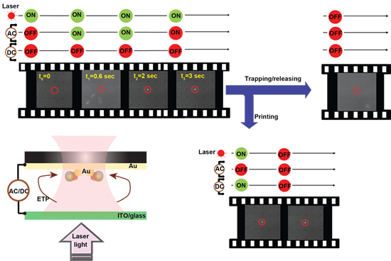
Hybrid Electroplasmonic Nanotweezer (HENT)
Plasmon-enhanced optical trapping is being actively researched as a means for stable trapping of nanoscale objects, which cannot be addressed by conventional diffraction-limited laser tweezers. In this approach, plasmonic nanoantennas are illuminated to generate highly localized and enhanced electromagnetic field in the vicinity of the nanoantenna. This highly enhanced and localized field also known as a plasmonic hotspot generates a tight trapping potential well for confining nanoscale objects. However a long standing problem in this field is how to rapidly load the potential well without relying on Brownian diffusion. Conventional plasmonic nanotweezer design rely on Brownian diffusion to load the trap, which is very slow and could take several minutes to hours depending on the concentration of the nanoscale objects. Recently we have addressed this challenge by introducing a novel design paradigm known as the Hybrid Electroplasmonic Nanotweezer (HENT), where a large scale microfluidic vortex is induced to enable rapid delivery and trapping of nanoscale objects within a few seconds. Furthermore we also print the trapped particles using a DC field, thus enabling additive nanomanufacturing functionality on-chip.
High Throughput Particle Concentration
Another aspect of this research focus on the use of closely spaced plasmonic nanoantennas arranged in an array. In this case, illumination of the elements in the array give rise to collective heating effect and a spatially distributed temperature field. With an applied AC electric field, volumetric body forces are induced in the fluid to generate a large scale microfluidic vortex. The vortex capture suspended particles and concentrate them with high throughput on the surface of the illuminated nanoantenna array.

Papers:
Glancing Angle Deposition
Contacts: Zhouxian Wang, Dr. Xiangeng MengAdvisors: Prof. Alexandra Boltasseva; Prof. Vladimir Shalaev
Collaborators: Prof. Alexander Kildishev
Short project description:
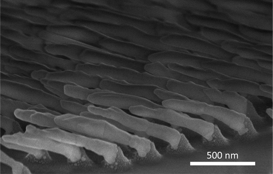
While conventional physical vapor deposition evaporators deposit material at near-normal angle of incidence, the Glancing Angle Deposition system allows thin films to be deposited onto three-dimensional structures with non-conformal geometries at very sharp angles (up to 90 degrees). Additionally, our evaporator is fully automated - with computer controlled 2 axes of rotation, deposition monitoring, and source selection. Automation of the system allows for the many multi-layer deposition required for the future generation of optical metamaterial devices.
One example of a sample fabricated with glancing angle deposition is shown below. This image shows the result of silver deposited on a 5 micron silicon sphere at a glancing angle. As can be seen in the image, a gradient thickness of silver is distributed along the surface of the sphere, with each thickness providing unique optical properties.
Papers:
Lasing with 3-D plasmonic nanorod metamaterials
Contacts: Zhouxian Wang, Dr. Xiangeng MengAdvisors: Prof. Alexandra Boltasseva, Prof. Vladimir Shalaev
Collaborators: Prof. Young L. Kim, Seung Ho Choi, Prof. Hui Cao, Dr. Sebastian Knitter.
Short project description:
Our nanolaser project aims to develop compact light sources using plasmonic nanostructures as resonant cavities. Here, we use an approach based on plasmonic metamaterials, composed of three-dimensional metallic nanorods (prepared by the glancing angle deposition, GLAD), to achieve plasmonically controlled random lasing. Our findings show that plasmonic metamaterials allow for the modulation of random lasing which may open up new avenues in nanolaser device design as well as fundamental science and spectroscopy. We are also interested in using other novel structures fabricated by GLAD technique and structures made of new plasmonic materials to achieve nano-scale coherent optical sources. The following figure shows a schematic of plasmonic random laser based on silver nanorod metamaterials.