OMEN

Within the next five to ten years the semiconductor industry will face the greatest challenge in its history. The conventional planar bulk MOSFETs will reach their physical and technical limit and the prolongation of Moore’s law will depend on novel and original device structures. For example the feasibility of silicon-on-insulator ultra-thin-body (UTB) and multi-gate nanowire (NW) field-effect transistors (FETS) has already been demonstrated by several groups [1,2].
Modeling such devices requires to go beyond the classical drift-diffusion approach and other effective mass approximation. The treatment of strong quantization effects as well as the atomic dimensions of ultra-scaled transistors is demanding state-of-the art physical models. For that purpose we have developed OMEN [3-5] the first atomistic and full-band quantum transport simulator designed for post-CMOS devices like UTB and NW field-effect transistors. A brief summary of its simulation capabilities is presented in this paper
Method
OMEN is a two- and three-dimensional Schrodinger-Poisson solver based on the sp3d5s* semi-empirical tight-binding method [6]. This bandstructure model has been chosen for (i) its ability to reproduce the principal bulk characteristics of electrons and holes, (ii) its straight-forward extension to nanostructures, and (iii) its atomic description of the simulation domain. Carrier and current densities are obtained by injecting electrons and holes at different energies into the device and by solving the resulting system of equations in the Wave Function or in the Non-equilibrium Green’s Function formalism [3]. The 2D or 3D Poisson equation is expressed in a finite-element basis where the tight-binding charges sit on node position. The computation of the bias points, the energy and momentum integrations, as well as the spatial domain decomposition have been parallelized so that a single simulation can run on a number of processors Ncpu up to O(10^4) with a speed-up factor close to Ncpu. As of November 2009 the code has scaled on Supercomputer #1 in the world, Jaguar at Oak Ridge National Lab, to 222,720 cores.
Geometry Examples.
Typical device structures that OMEN can handle include NW field-effect transistors with any cross section shape (square, circular, triangular, hexagonal, .....), gate architecture (all-around, single, double, or triple), and transport direction (<100>, <110>, <111>, <112>, ...) as well as UTB FETs with single- or double-gate and any configuration of surface orientation and transport direction. Different semiconductor materials have been parametrized, among them Si, Ge, GaAs, InAs, AlAs, or SiGe. Ternary alloy semiconductors like InGaAs and AlGaAs are treated either as virtual crystals or as atomistically and randomly disordered entities [7]. The multi-level parallel implementation of OMEN and the optimization of its numerical algorithm make the simulation of NW with a cross section up to 22 nm and UTB with a body thickness up to 8 nm and a realistic gate length of 22 nm possible.
Application Examples.

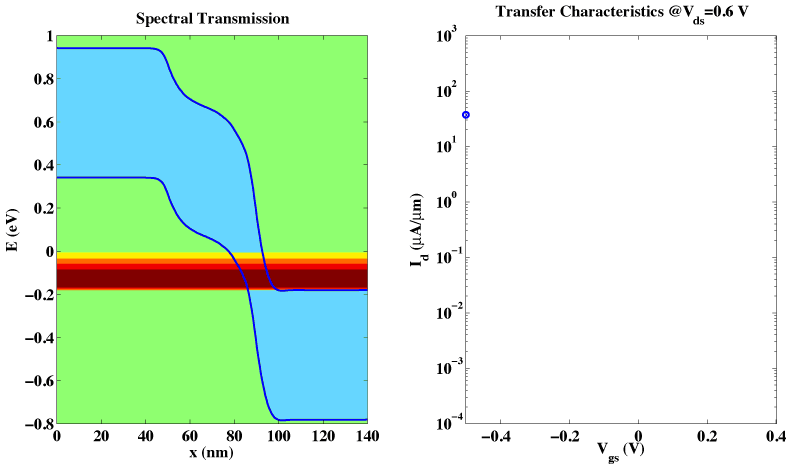
- Gate Control and Sub-Threshold Swing in BTBT
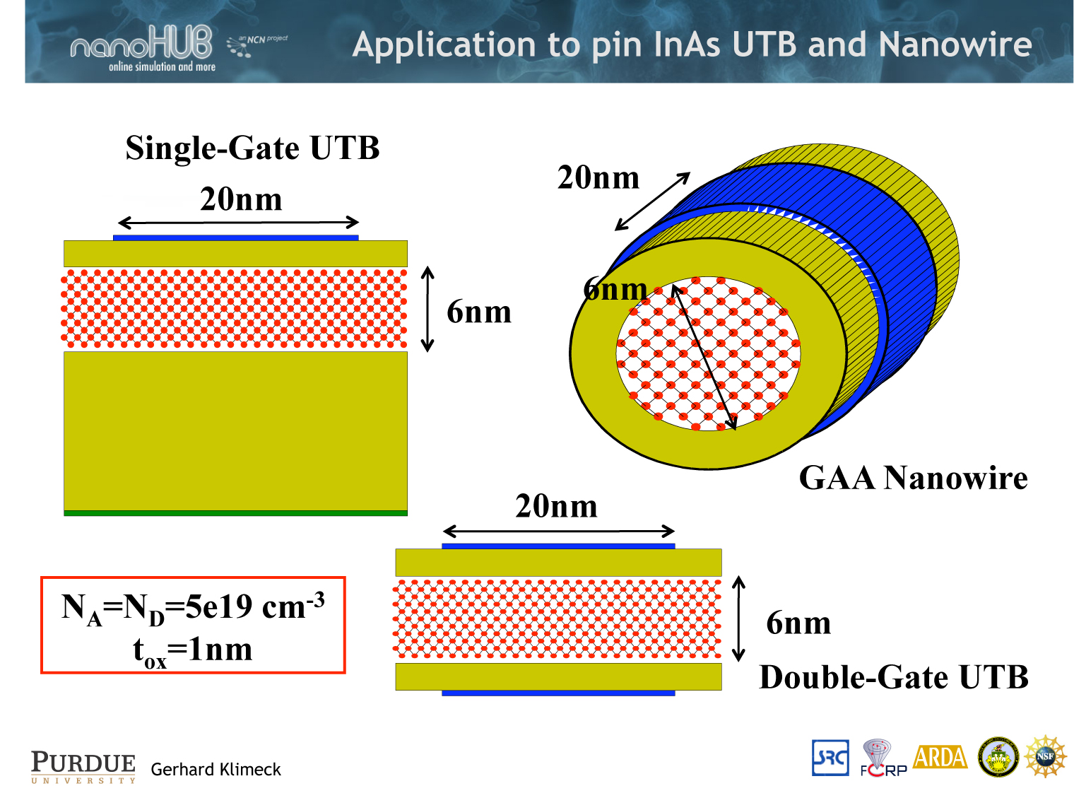
- Comparison of in pin InAs Devices – SG-UTB / DG-UTB / NW
 .
.
- Comparison of in pin InAs Devices – SG-UTB / DG-UTB / NW