Jennifer Tietz' Lab Notebook
Week 01
January 10, 2006 (1 hour):
This was the first day of class. We solidified our team, as well as a
clever team name, the J Team. We had a team meeting to brainstorm possible ideas for the design project. Some
of the ideas that we considered were an IPASS unit that had additional built-in capabilities, a digital host
for use in a restaurant, a laser tag game, and a laser target practice unit. The team decided to do additional
research on Josh's digital host idea. He had a personal interest in the project since he works as a host at
Chili's. Our initial concern was that the project might be too software-intensive, and the solution we would
develop for this course wouldn't be nearly as practical as developing a software suite to do the same thing.
January 11, 2006 (1 hour):
Today we had a team meeting to expand on the research we had done for the
digital host project idea. Josh brought a list of applications & interfaces for the "DigiHost", and we
discussed different peripherals with which we could interface.
At this time, Jared shared with the team an
idea that he had thought of for an RFID checkout system in a supermarket. He envisioned a shopper filling up a
shopping cart with numerous items tagged with passive RFID tags. Shoppers would apply for an RFID Key Fob
to attach to their keychain that contained an identifying unique user number. When finished, the shoppers would
pass through the exit door, on which would be mounted an RFID receiver. The receiver would read all of the tags
simultaneously, as well as the shopper's keycard or FOB that would act like a SpeedPass. An email receipt
would be sent to the shopper, obtained from a database accessed via the shopper's user number.
The team
members really took well to this project suggestion, as we thought of many different possibilities for
interfacing and considered this topic to be a valid step forward in potential future technology. We decided to
do more independent research on RFID applications, since none of us had any previous experience. Jared and I
both helped to develop concept appliance ideas with Whirlpool Corporation in the Summer of 2005 during our
internship there, which was the source of the idea.
January 12, 2006 (1.5 hours):
I spent a bit of time this afternoon surfing the internet for
information on RFID technology to gain a better understanding. Huge learning curve for me today!
Helpful sites that I used for reference:
http://www.rfidjournal.com/faq
http://www.ti.com/tiris/docs/customerService/faq.shtml
January 12, 2006 (2.5 hours):
Today's team meeting centered mainly around drafting our initial
project proposal, which was due tomorrow. We did an ample amount of online research as a team to learn the
fundamentals behind RFID applications. We searched for possible development kits or chips, but we're unsure as of
right now whether we are expected to just buy a kit or build the receiver/transmitter/antenna ourselves.
That seems a bit hardware-intensive, and quite frankly, with a group of 4 software-oriented CompEs, scares us!
During one of our many Google searches, we happened upon a 477 Senior Design Team's website from about a year
ago who attempted a similar project. We were able to snoop around and gain some insight as to how they chose
to approach their project. We were a little worried by the fact that their project seemed to be
unsuccessful at the end of the semester though!
We learned that for our project, we would most
likely need to use high frequency tags and readers (13.56 MHz) in order to obtain the maximum range (up to
3 feet, according to the websites above). Unfortunately, antennas for that range are quite
expensive! We wonder just how generous sample parts givers can be. Finally, we completed our initial project idea,
which can be found here. We also divided up the responsibility for the Design
Component Homeworks and Professional Component Homeworks.
WEEK 01 SUMMARY
Accomplishments: Formed design team, decided upon a seemingly appropriate project idea, researched
fundamental concepts of RFID technology and systems, drafted an initial project
idea proposal for course staff to review, determined areas of project responsibility.
Weekly Work Total: 6 hours
Project Work Total: 6 hours
Week 02
January 18, 2006 (2 hours):
Today we received our initial project idea back in class, and Dr.
Meyer provided some useful feedback about his perceived difficulties with the RFID tag detection and
differentiation. The course staff said our projet was not "tractable". First we spent some time investigating
the concept of tag collision, which is when multiple tags, or tansponders, emit a frequency at the same time,
confusing the reader. This problem was anticipated in our project since many items in the cart will all be
transmitting simultaneously. We learned that while several companies have developed algorithms for
anti-collision that singularize the tags so they appear to send data one at a time, this technology is new and likely
underdeveloped. Rather than experiment in such a gray area for our senior design project, we brainstormed
methods to modify our project idea so that tags were being read one by one. We came up with two modifications:
the first was an RFID garage door that detected tags on the license plate and opened for correct cars only, the
second was a Walmart-like self-checkout system using RFID technology as opposed to the current UPC. The team
seemed unanimously pleased with the later idea, as it was closely related to our initial project idea and
completely resolved the issue of tractability.
We also ran across several websites that discussed practical implementations of our new idea:
Self-Checkout Gets RFID Upgrade
Self-Checkout Popularity Increasing
January 19, 2006 (15 mins.):
After class today, our team spoke with Dr. Meyer about our proposed
change to our initial project idea, and he approved it. We are happy to finally have an official project!
WEEK 02 SUMMARY
Accomplishments: Researched RFID technology and appliations, brainstormed related project ideas, settled
on self-checkout RFID system, had new project idea approved by Dr. Meyer.
Weekly Work Total: 2.25 hours
Project Work Total: 8.25 hours
Week 03
January 24, 2006 (1 hour):
Jared, Josh, and I met today to discuss our 5 Project Specific Success
Criteria (PSSC). Tomorrow in class, we will give a 1-slide PowerPoint presentation of our 5 PSSC to the class. We
decided upon the following initial PSSC, to be evaluated and modified by classmates and course staff tomorrow:
1. Ability to provide audio feedback ("beep") in response to RFID detection
2. Ability to display useful information on LCD
3. Ability to email customer a receipt of purchase
4. Ability to identify an item by reading its RFID tag
5. Ability to interface with a keypad to input customer PIN
We then designed our custom powerpoint background and organized our brief presentation for tomorrow. Our
PSSC presentation can be found here, as well as on the "Documents" page.
January 25, 2006 (2.5 hours):
The team met today after class to make the suggested revisions to our PSSC, as
seen below (reordered & reworded):
1. Ability to identify an item by reading its RFID tag
2. Ability to enter customer PIN on a keypad for added security
3. Ability to modify the product database via an embedded web server
4. Ability to display useful information on a graphical LCD (e.g., customer ID, scanned item description, etc.)
5. Ability to email customer a receipt of purchase
We also worked to develop a general block diagram so we could
better visualize the components of the project, which Jared helped out with a lot. Afterwards, I spent a while
working on revising our initial project idea from homework 1 for the Project Proposal, or homework 2. Jared and
I explored our new plan to purchase a multi-frequency RFID module that contained a reader and an antenna, rather than
trying to buy the reader IC and build an antenna, as we had previously considered. This solution seems much more
practical!
January 26, 2006 (3 hours):
Jared and I searched the internet for more specific products that met the
design constraints for our project. Our initial aim was to gain a better price estimation for the prototype;
however, we ended up learning a lot more about the options available to us and simplifying our existing block
diagram (for example, we were able to remove a keypad controller and LCD controller). I created the block
diagram, finished writing the Project Proposal for homework 2, had it read and
approved by the team.
Here are some of the components that Jared & I found this evening:
neCore12 MC9S12NE64 Microcontroller w/
10/100 Ethernet, $67.00
TI S4100 Multi-Function RFID Reader
Module, $90.00
Crystalfontz 320x240 negative
blue backlit graphic LCD, $145.00
Storm 16 key
keypad, $45.00
70dB 2.048kHz
magnetic external drive buzzer, $1.00
TI Tag-it HF-ISO Mini Inlay
RFID tags, $1.55/ea
TI Tag-it 13.56MHz ISO Vicinity
Key Ring Transponders, $6.00/ea
WEEK 03 SUMMARY
Accomplishments: Developed acceptable PSSC and presented to classmates and course staff, completed Project
Proposal, corresponded with Symbol reps about requests for demo parts, selected several
candidate components.
Weekly Work Total: 6.5 hours
Project Work Total: 14.75 hours
Week 04
February 1, 2006 (2 hours):
We had a team meeting over lunch today to discuss the estimated cost of the product
and come up with a plan to start requesting sample parts. Jared and I explained our choice of the microcontroller to the team,
and they agreed with our decision. At least for now, we can't forsee the need to spend more money just to obtain more pins
and built-in peripherals that our application won't make use of.
As for the requesting of sample parts, we staggered our phone calls and emails so that the companies
wouldn't be bombarded by multiple requests for the same part from one team. I was assigned to email TechnologicalArts
about our microcontroller module and special development board. The Micro retails for $79 and the dev. board for $48.
We found out in their response email that they don't give sample parts, but offer a 15% educational discount, which would
bring those prices down to $67.15 and $40.8, respectively.
I also gathered information about Homework 3 and Homework 4, which are due next Friday. The papers are assigned to Josh and
Jonathan, but we're hoping to work on them as a group. On a bad note, Josh found out during his conversation with a TI rep that
the reader module that we had selected actually doesn't include an antenna. I guess the documentation is a bit misleading, because several
of us read it and thought that it did include an antenna adjustable to short and long range frequencies. This
means that we're going to have to work extra hard at finding an affordable one, or rather, a very generous supplier.
February 4, 2006 (3 hours):
Today I did lots of online research attempting to locate similar products that we can compare our project
to as part of the Homework 3 and Homework 4 requirements. Not only was it difficult to find such products, but it was even harder to find a MSRP
for them. I guess this is understandable since the self-checkout system is a commercial product, so generally all that interested people need is a
contact with the manufacturer. I've sent emails to the manufacturer of both of the products below, hoping to hear back on a standard price.
The most similar product that I found was the NCR FastLane, which has
actually been installed in Metro Group's RFID Innovation Center in Neuss-Norf, Germany, a sort of "grocery store of the future". This product is
actually the entire checkout station, but it uses UPC labels to identify the products and deactivates RFID tags on the products to enable them to
pass through security without beeping.
It took a long time for me to locate a second product that was similar to our project. I really wanted to locate the manufacturer of the
self-checkout lanes at WalMart, since those most closely match our design, even though they use UPC labels instead of RFID tags on the purchased items.
However, I learned that the company that originally made those, Optimal Robotics, sold its self-checkout business to Fujitsu Transaction Solutions
in 2004. Their product, called U-Scan, also consists of the
entire checkout station.
Finally, I found a third product that actually utilizes RFID technology, but in a different way. This product, called
XpressCheck, is a self-service kiosk designed for use in a library. It
deactivates RFID labels on multiple books "simultaneously" to enable them to pass through security.
February 5, 2006 (1 hour):
I started helping Josh and Jonathan today on Homework 3 and Homework 4. I did some additional research on
the NCR and U-Scan units, and wrote the Cost Constraints section of Homework 3 & sent it to the group for approval. I hear back from the NCR rep
today... she said that due to company policy and security reasons, they cannot release pricing information for the FastLane. I still haven't
heard at all from Fujitsu, so I'm beginning to assume they're in the same boat. I also learned that only the FastLane installed in Germany is
fitted with the RFID upgrade kit - it doesn't come standard yet. This is important to note in Homework 4 when we're doing the product comparison -
RFID Expr3ss will be the only product of its kind on the market!
WEEK 04 SUMMARY
Accomplishments: Acquired multiple sample parts, including microcontrollers, development boards, and keypad, found several simlar
products available for comparison, began work on Homework 3 and Homework 4.
Weekly Work Total: 6 hours
Project Work Total: 20.75 hours
Week 05
February 7, 2006 (3 hours):
This was our first team meeting to help Jonathan and Josh get started on Homeworks 3 and 4, respectively.
Everyone came with bulleted points of information that they thought should be discussed in each section of the paper. Jared and I agreed to take
responsibility for the PowerPoint presentation due tomorrow for the TCSP on Design and Packaging
Constraints, as well as the PCB Footprint Layout (since we are working on the schematic and PCB for Homeworks 5
and 6). We also made final decisions on component selection, including changing
our reader to the Intersoft reader/antenna and tags and Fobs (Josh is in contact with
a rep. there to find out more information, as their online documentation is a bit lacking) and selecting a
Storm 16-key keypad as opposed to the Grayhill one that Jonathan procured for us for free. The Grayhill pad just
had a cheap look and feel to it, with hard-to-press, small buttons... not ideal for a consumer application where the PIN is entered from a
distance.
February 7, 2006 (2 hours):
Worked with Jared to design the TCSP and gather information for the component selection and packaging while
Josh and Jonathan worked on their respective papers. Then Jared & I loaded the Orcad software on the home computer and experimented with Layout.
Unfortunately, it isn't the most intuitive software. We had a hard time finding the exact specs for our parts in the data sheets, but once we did,
we had an even harder time finding the parts in the libraries. And then there was figuring out how to move them from being right on top of each
other... LOL. Either way, tonight was a good learning curve with respect to that software, and we feel much more comfortable about having to
work with it on our upcoming homework.
February 8, 2006 (0.5 hour):
Today we had our TCSP in class, and Jared & I went to Nick's office
hours to talk to him about PCB Layout issues. He explained to us how we can add pins to existing parts, and gave us some ideas on design
constraints, such as minimizing board size and footprints, heat considerations, and RFID range (the later two of which we have already thought
about). We talked a bit about TCP/IP as well and anti-collision technology that we might want to incorporate into our software design.
February 8, 2006 (3 hours):
Tonight I spent a long time editing Josh's paper, Homework 3. He had most of it written already, so all we
had to do was fix up stuff and make sure it agreed with what Jonathan's paper said. Either way, a really long night.
February 9, 2006 (3 hours):
Jared and I spent tonight much like yesterday, except this time we were editing Jonathan's paper. His was
considerably longer and had more technical details, so it took a good amount of time. He hadn't written all of the parts yet, so we helped with
the conclusion and the interface requirements section.
We also received feedback today from Dr. Meyer about our Project Proposal and PSSCs... looks like we're going to be doing a bit of changing
those around and adding a printer! It was too late to incorporate those learnings into these homework assignments, though. Maybe later.
Final copies of the submitted homeworks can be found in these links:
Homework 3
Homework 4
WEEK 05 SUMMARY
Accomplishments: Finished HW3 & HW4, completed TCSP on Design and Packaging Considerations, made final decisions on component
selection, procured more parts, completed PCB footprint, contacted more vendors, researched printer parts.
Weekly Work Total: 11.5 hours
Project Work Total: 32.25 hours
Week 06
February 17, 2006 (4 hours):
I spent a long time working on the schematic today and actually made significant
progress. Jared showed me how to customize parts (as he had done for the uC), so I was able to lay out the Ethernet circuitry, oscillator,
and most of the RFID connections (which consists of a DSUB9 connector the RS232 level traslator). After working on it all afternoon, I had
accumulated quite a list of questions, which I emailed off to Brian and Nick.
Josh and Jonathan went to office hours this afternoon to learn how to do a power supply design. Since all four of us are CompE's, we were
really in the dark about that part, but Nick made it sound easy. Our only problem now is that we seem to have more supply voltage needs than
they originally estimated, since we need 3.3, 5, and 9V (the printer will run on approx. 12V I think).
We also had our design meeting on Wednesday with Dr. Meyer and company. I think it went really well as they didn't seem to have any
pressing questions or concerns. We should be getting our 9S12NE64 demo board for the semester from Chuck, since
the two boards that Josh was approved for never arrived. We also ordered all of our major components for the
project on Tuesday, most of which have already arrived.
February 18, 2006 (5 hours):
Jared and I spent a long time finishing up the Orcad schematic today. Nick
and Brian got back to us pretty quickly with answers to my questions. Most of my trouble came when trying to
determine which of two seemingly identical components to select in Orcad, such as for the 25 MHz crystal
oscillator and the DB9 connector. We still have a few lingering questions that the TAs weren't able to resolve:
1. Our LCD has a Vee pin that we're not sure what to do with; Nick suggested that it was for the backlight,
but we've already supplied the +/-5 V required for that.
2. Our MAX233A level translator has an "Internal +10 V Power Supply" pin that we're not sure what to do
with; we've already supplied the +5 V power supply for the chip. Nick suggested that we follow the application
notes as closely as possible for our design, but the data sheet doesn't go into detail about the internal
power at all.
After completing all of the net aliases and organizing the schematic in the most visually-appealing way
possible, we generated the netlist (which passed all the design rule tests!) and found a major setback - we hadn't
used surface mount components for all of our resistors and capacitors, and as a result, there were no footprints in
Layout available for those and other headers and miscellaneous parts. After correcting this problem by changing
all of the resistors and capacitors, we generated the auto-layout in Layout. We then started making custom
footprints for all the components, starting with the RS232 connector. The datasheet was helpful, but some of our
other ocmponents are not as well documented online.
Follow the link below to find an image of the current schematic, v1.0:
Orcad Schematic
February 19, 2006 (2 hours):
Tonight I started on the Homework 5 paper, which is my responsibility.
I wrote the introduction and made a skeleton for the summary. The schematic has come along considerably well and
we are learning more about Layout every day. I haven't yet added the power supply
circuit into the schematic... all the supply voltages are simply marked with their required values.
Tomorrow Jared and I are meeting Chuck to get our demo board for the semester and picking up the last
of our ordered parts which seem to have arrived in the mailroom!
WEEK 06 SUMMARY
Accomplishments: Ordered all major components, had first design review, completed Orcad schematic,
began writing Homework 5.
Weekly Work Total: 11 hours
Project Work Total: 43.25 hours
Week 07
February 21, 2006 (1 hour):
I met the team in the lab today so that we could hopefully get some questions
answered about our power supply design, as well as learn more about how to route parts in Layout. For the power
supply, we've been struggling with the need to produce 3.3, 5, and 9 V supplies. Our printer comes with its own
12 V wall-wart, which we were advised to let be, and use a separate wall-wart for the rest of our needs. However,
with the voltage regulator chips that Jared was looking at that take in 12 V and reduce it to 3.3 and 5, we would
dissipate something like 5 W of power! We spoke with Dr. Meyer about doing a step-up DC/DC converter, so Jared is
doing some research on that - he found some TI parts to sample that we think might do the trick.
As for our questions about Layout, I think the team is just frustrated right now because none of us has
experience using Layout and exactly how to use it hasn't been spoken about in class at all. Thankfully, we found
the tutorials to be very helpful.<\p>
February 21, 2006 (9 hours):
Tonight I got a significant start on the Theory of Operation section of
Homework 5. It really is a lot of work searching through all of the datasheets we've compiled and explaining
the operation of all the pertinent signals. I have some holes in the paper, mostly that I have to clear up with
Jonathan. He was in correspondence with Star Micronics to get us the thermal printer, and they sent us a 7 V DC
regulated power supply when the data sheets say that the printer requires 8 - 13 V. I guess we'll have to contact
them again and see if they know something that we don't.
I also spent a good amount of time working on the TCSP for tomorrow. Taking images of the modules of
the schematic was actually helpful because I found a few minor errors that we had to correct. As of now, the
schematic at least looks complete, with the exception of the power supply circuit.
The PCB is still a rat's nest right now, but we've been working hard on designing custom footprints and, as I
explained, still have many questions about routing that we need to get answered.
February 22, 2006 (6 hours):
The team met in the lab today to accomplish many different tasks. I spent
nearly all of my time writing and completing HW5. I posted it on the site tonight so the team
can read it and provide feedback sometime tomorrow. Jared worked very hard on the PCB Layout and pretty much
started over from scratch again. Nick was a good help to us today, and seeing some other teams' PCB Layouts today
in class for our Schematic and PCB Layout TCSP gave us a much better idea of what we should be doing. We learned
that the RFID tags and key fobs actually have about a 4 - 5 inch range, which is right about
what we expected.
Here is our completed Homework 5 and Schematic
and PCB Layout TCSP.
February 23, 2006 (2 hours):
Tonight I worked with Jared to help him write Homework 6 about the
PCB Layout Design. We actually learned of some additional considerations as we were researching for the paper,
so I guess we'll have to include those in our successive iterations of the PCB (which we're sure we'll have to
do). Jared also helped me with editing my paper. Luckily, we were also able to clarify the confusion
over the power supply for the printer - even though the documentation says it requires 8 - 13 V, the
rep for the company says that the printer only needs 7 V because the actual active range is 6 - 14 V. So
at least we think we've finally finished the power supply design for good!
I also prepared a Design Project Change Order Request to be submitted tomorrow in order to change
our PSSC #5. Dr. Meyer had originally written our PSSC #5 as: "An ability to store a local copy of the
product database in non-volatile memory, and update the database via an embedded web server." The team's original
plan was to have an on-chip database; however, after considering the ideal implementation of our system if it was
to be widely used within a supermarket, we decided it would be better to move the databases off-chip. Thus,
we proposed our new PSSC #5 to read: "An ability to gather product and customer data by querying an external
database (using Ethernet)." The actual wording of this new PSSC was discussed with Dr. Meyer in class a
week or so ago, so we don't really have any doubt that it will be approved.
Here is our completed Homework 6 and an updated copy of our
PSSCs.
WEEK 07 SUMMARY
Accomplishments: Finished power supply design, gave Schematic and PCB Layout TCSP, completed Homework
5 and Homework 6, finished initial PCB layout, submitted Design Change Request for
PSSC #5 to move customer and product databases off-chip.
Weekly Work Total: 18 hours
Project Work Total: 61.25 hours
Week 08
February 26, 2006 (5 hours):
Tonight I got started on the Formal Design Review Presentation for
later this week. I basically filled in all the slides except the packaging design one... I'm not
really sure what we're going to put there yet. Josh did the packaging design paper, but his CAD drawing
is not at all up-to-date because we didn't have the printer incorporated into our design yet. I'll
probably just ask him to do this slide.
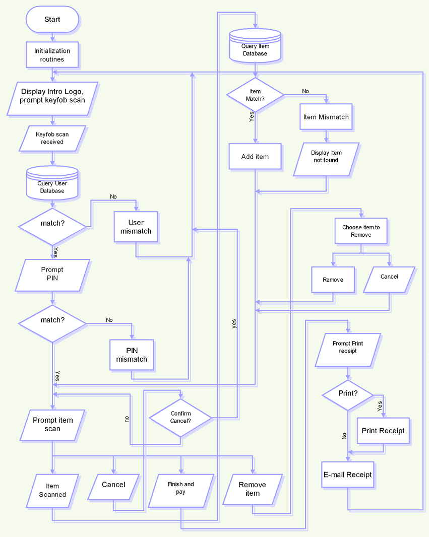
Jonathan and I worked on developing a flowchart for the software logic. I was actually surprised
at how simple it seemed to be. Most of the design is interrupt-based (keypad, RFID), so our main
program is largely just "waiting" for some event to happen. Jared put the flowchart into the computer
so we have a digital copy.
I also made a new block diagram for our overall design, based on suggestions that Dr. Meyer
mentioned in class. It is much more specific now, with bus lines labeled with their widths, which is
something we couldn't have done on the original block diagram anyway because our components were not yet
selected.
Some fruits of my labor tonight:
System Flowchart
New Block Diagram
February 27, 2006 (6 hours):
Jared and I worked today making minor updates to the schematic
and PCB, and I completed the rest of the presentation slides needed for our Formal Design Review tomorrow.
I spent a lot of time practicing since the 35-minute timeline is pretty rigid.
The masterpiece:
Formal Design Review
February 28, 2006 (5 hours):
Today was the Formal Design Review. Dr. Meyer, Nick, and Brian made many suggestions about modifications
to our schematic and PCB, so Jared and I made lots of progress on them today. Nick suggested that we
remove the keypad encoder and just wire the 8 keypad pins to the uC (since we have so many unused I/O pins)
and code it in software. This should save us space on the board by getting rid of the IC. Also, the
micro has internal pull-ups and pull-downs that are programmable, so we are able to remove ALL the SIPS...
that will free up lots of space and make rerouting much simpler for Jared and the PCB.
They made some more really good points that we looked into - Brian was concerned about the voltage
swing on the LCD, at 5 V, obtaining its signals from the 3.3 V micro. We checked the data sheets and found
that for the LCD, V_IHmin = 2.2 - Vdd, and for the micro worst case, V_OHmin = Vdd - 0.4 = 3.3 - .4 = 2.9 V. So,
we won't need a level translator in between.
Since we hadn't actually ordered our discrete parts yet, Nick pointed out that some of our footprints
on the PCB were too small, such as for the caps on the power supply and the 25 MHz crystal. I guess our team
hadn't been too concerned about ordering discrete parts yet because there were supposed to be many available
at the window, and we didn't actually need to do the parts acquisition until the Friday before spring break.
After the presentation though, we decided that we might as well order the parts if we know what we need,
so Jared and I spent the evening searching DigiKey and ordering them all.
Jared is also going to work on rerouting the PCB, since Nick and Brian informed us of more
design considerations to take into account. Our Ethernet circuitry is still too far away from the micro,
which surprised us since the traces on the 9S12NE64 dev board that we got from Chuck aren't incredibly short and we felt
ours were comparable. Nick also said that traces should overlap at 90 degree angles in the Ethernet circuitry,
so we're going to try to work on that. Oh yeah, and apparently we didn't create a net for our copper pour
underneath the voltage regulators... oops.
March 4, 2006 (5 hours):
Jared, Jonathan, and I met in the lab today. Jonathan worked on the
software to try to understand more about Code Warrior. Apparently there is a file missing from the installation
that is required for the NE64.pe. After installing an updated version of Processor Expert, we were able to find it.
It ended up being a waste of time though because we have since decided not to use Processor Expert for the start-up
code. Jared and I sorted through all of the discrete parts data sheets to make new custom footprints for the
larger pieces, such as the polarized caps, the inductors, the Schottky diode, and the crystal. We placed all the
footprints on the PCB, but haven't started the routing yet, hoping to get homework feedback soon.
WEEK 08 SUMMARY
Accomplishments: Prepared for and delivered Formal Design Review, updated schematic according to
Design Review suggestions, ordered and received all discrete parts, began revisions on
PCB.
Weekly Work Total: 21 hours
Project Work Total: 82.25 hours
Week 09
March 7, 2006 (2.5 hours):
Jared and I went to Brian's office hours today to ask him some final questions
related to the PCB. We are having difficulty finding a 1500 pF polarized cap for the power supply circuit. Since
the capacitor merely connects a pin to ground, Brian told us we didn't need a polarized one, so we were able to get
one from the lab. We were also concerned about whether our DB9 connector was of the right gender - the printer
comes with a male end, and we're making the RFID connector from scratch, but we currently have two male footprints
on our PCB. Brian said it didn't matter if we put gender changers on the connectors or not.
We later made a few updates to the PCB routes and change the pin orientation on
the header for the LCD on the schematic. Since our PCB was fully routed and finished, we decided to do our
Parts Acquisition and Fit early with Brian. He checked us off for everything. We have made a few modifications
after that, merely putting labels on the silkscreen. Tonight Jared and I are going to redline the PCB before
we submit it to www.freedfm.com.
March 9, 2006 (2 hours):
Jared and I redlined the entire PCB design with the schematic prior to
submitting it, and were glad that we found no errors. We then submitted the PCB to www.freedfm.com, though we had
some difficulty determining how to label some of the files (i.e., which ones were "NCDrill" and what to do with those
that didn't match any options... we put "other" in most cases I think). The results came back that we had around
200 "autofixable" errors, which Brian told us had already been taken care of. Nearly every one was the result of a
problem with the solder mask.
Some updated documents:
RFID Xpress Schematic v4.0
PCB submission, top copper
PCB submission, bottom copper
WEEK 09 SUMMARY
Accomplishments: Completed Parts Acquisition and Fit (HW7), redlined schematic and PCB, submitted PCB
to www.freedfm.com and emailed it to Chuck.
Weekly Work Total: 4.5 hours
Project Work Total: 86.75 hours
Week 10
March 19, 2006 (6 hours):
Jonathan, Jared, and I went to the lab today to continue working on software
development. Since we have now acquired a BDM connector that actually works (3.3V instead of 5V) from Chuck, we
were able to upload the startup code to the uC and run some demos. Right now we're having difficulty controlling
some of the output pins on Port G and Port S... when we connected a 7-seg. LED to do some debugging, we were
getting erratic output. We thought it might be a problem with the DDR bits, especially since Port S is typically
used for serial communication, but we disabled all of that in the control registers. We eventually built a prototype
for the keypad, with its 4 row lines on PTS0-3 and 4 column input lines on PTS4-PTS7. We then wrote a piece of
code using the following simple algorithm:
1. Assert first column, leave all others low
2. Scan each row in that column to see if one is asserted; if yes, output key number to 7-seg LED
3. Repeat steps 1-2 for remaining columns, loop infinitely
We were able to successfully identify some key presses, and found the problem... PTS0 seems to be
driving 3.3V to the keypad as opposed to being an input to the uC. This is contrary to how we have our DDRS
register set, so we're going to work on this problem again later.
Code Listing:
Keypad Polling Code
WEEK 10 SUMMARY
Accomplishments: Ran startup code on uC, prototyped keypad, generated preliminary keypad code.
Weekly Work Total: 6 hours
Project Work Total: 92.75 hours
Week 11
March 21, 2006 (1.25 hours):
Today Jared and I completed our prototyping of the PIN entry pad. We still
could not figure out why the PTS_PTS0 port is driving 3.3V, and neither could Brian. So, we moved the row input
lines to Port J, which worked as expected. We are now able to correctly identify which key is pressed.
We also added code to compare a 4-digit PIN entered by the user with one stored in memory, and to illuminate
a blue LED if matched and red LED if not. We realized that the fast speed of the polling was registering
many digit inputs when the user just pressed one button, so we added functionality to only capture one key press
per key release. We also removed the 10 kOhm pull-down resistors we were using on the row inputs and programmed
the internal pull-downs on the uC.
At this point, we're not concerned about the problems with the SCI Port 0 on the demo board since our design will
actually implement SCI communication through both SCI ports (as opposed to using it for general I/O, as we
were trying to do in this case) on the microcontroller.
Code Listing:
Keypad Polling Code with PIN Verification
March 22, 2006 (3 hours):
We accomplished a lot in lab today related to the serial communication. Jared
and I began prototyping the RFID reader using the SCI Port 1 on the evaluation board instead of the demo board that
we had been using. Previously, we were having trouble with the Port S0 bit, as it was driving the output high to
3.3 V. However, the SCI port responded accurately when we used the eval board. We were able to generate code to
detect the RFID serial number and display it to Hyperterm. One problem that we predicted actually came true - the
9600 baud rate to transmit bits, combined with the speed of scanning by the RFID reader, actually cause the reader
to detect the same tag multiple times (usually between 1 and 4) for each time it is "passed" over the reader.
However, I have multiple ideas of how to handle this - the first and easiest of which would probably be to store
the most recently scanned RFID serial number in memory and only register a "detection" of a tag if it is different
from this previously scanned serial number.
After our success with the RFID prototyping, we began working on the printer, which also utilizes the SCI
Port (0). Programming the memory switches on the printer was a very interesting task, but the online documentation
was extremely helpful. We set 3 of the 16 switches to be "ON" - the first (S1-1) set the communication protocol as
serial instead of USB, the second (S1-7) set the flow control to XON/XOFF so that no handshaking was necessary,
and the third (S2-1) set the character set to be USA standard (which is actually considered overseas, not
domestic).
We wrote a function to send the RFID serial number bits that were scanned directly to the printer,
which worked well for the most part. The only anomaly that we experienced was a single digit that was printing
out prior to the start bit (a colon) of each RFID serial number... the digit varied from 3 to C to B to 6 in a
seemingly random fashion - I'm wondering if there is something wrong with our baud rate (which was published
directly in the printer documentation) or if those characters are simply stuck in the buffer somehow. We were
happy to realize, though, that those random preceeding digits only appeared when we were transmitting the RFID
data directly to the printer; whenever we programmed specific text to be printed (such as the logo we made for
the top of all the receipts), the digits never appeared.
Code Listing:
RS232 Serial Communication Code
RFID and Printer Prototyping
March 24, 2006 (4 hours):
The team met in lab today to work more on the Ethernet code and the PCB. Our
board came in yesterday, so I completed "Ohm-ing out" the traces and inspecting it under the microscope -
everything looked to be fine. Jared and I worked together to solder on the power supply circuit and test the
voltages. We are getting very clean 3.3, 5, and 12 V signals thus far, but we are going to leave it on for the
night to burn in the circuit.
We found one slight error on our PCB - the footprint for C27, a 100uF capacitor,
was too small. Another cap, C30, is the same value and had a much larger footprint. Luckily enough, we were
able to find another 100uF electrolytic capacitor in the lab that was smaller than the one we ordered from
DigiKey. It is still quite a tight fit, but we were able to solder the pins and have a nice signal across the
cap.
March 25, 2006 (2 hours):
Today we went into lab to check on the power supply circuit and work more on
the Ethernet code. The power signals still looked good, so I continued populating the board by soldering on
all of the bypass capacitors. After doing so, the signals were verified again, and power was being provided
accurately to all the ICs. I also helped Jared with the Ethernet code, since we are still having problems
establishing a link when using the BDM (since the auto-generated code from Metroworks utilizes the serial port,
both of which we are using in our design). We were able to successfully load the code using the BDM after getting
some tips from James Doty. Later, Josh and Jared were able to spoof an ECN computer on the uC, so we are
confident that we've finally figured out how to connect to the internet.
WEEK 11 SUMMARY
Accomplishments: Completed keypad, RFID, and printer prototyping, populated power supply and bypass caps
on PCB.
Weekly Work Total: 10.25 hours
Project Work Total: 103 hours
Week 12
March 28, 2006 (2 hours):
Today the team met in lab to make more progress on the software development.
While Josh and Jared worked on the Ethernet code, I made our first
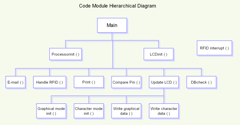
Code Module Hierarchical Diagram (made into digital work by Jonathan later that night).
After sketching it out, I began writing a hybrid of code/pseudocode on my
implementation for the main, HandleRFID, PollKeypad, PrintReceipt, and EmailReceipt functions. I also worked with
Jonathan to make modifications to his upgraded Software Flowchart.
March 28, 2006 (3 hours):
Tonight the team met to prepare for the
Software Narrative TCSP tomorrow. We
had several design decisions to make, as all of the code we've developed thus far has been modular (and we didn't
really need to decide how the implementation would work at that time). Our checkout design will be controlled using an
"Interrupt-Flag-Driven-Polling-State-Machine" algorithm. The main program will loop through a series of states
(some examples include "IDLE", "PIN ENTRY", "ACTIVE SESSION", "RECEIPT", "PRINT/EMAIL", etc.), and depending on
the state, will check if a particular flag has been set by an RFID interrupt, keypad press, or an LCD change request.
If that flag was set, then that condition will be handled, the flag cleared, and the state updated. Prior to looping again,
we will verify if a keypad entry is expected in this state; if so, then we will poll the keypad and capture any
data, setting the keypad press flag.
We also decided upon how we will handle an RFID interrupt. We concluded that data on the SCI1 port will
trigger the RFID interrupt, and the ISR will simply set an RFID flag. Inside the main loop, if the flag is set in
a particular state, the HandleRFID() function will be called, where we will strip the serial number off of the SCI1
port and into SRAM. We had previously entertained ideas of storing the serial number in memory during the ISR, but
concluded that this other method of handling would coincide better with our general organization of quick interrupt
service routines and handling within the main loop.
March 30, 2006 (4 hours):
Jared and I worked with Jonathan to help him write the software narrative
paper. Specifically, we discussed implementation issues with the LCD and RFID interrupt handling. I also edited
Josh's paper as well.
Our most recent homework assignments:
HW9: Patent Liability Analysis
HW10: Software Design Narrative
WEEK 12 SUMMARY
Accomplishments: Completed Software TCSP, finalized general software organization, helped complete
HW9 and HW10.
Weekly Work Total: 9 hours
Project Work Total: 112 hours
Week 13
April 4, 2006 (5.5 hours):
The team met in lab today and really made decent progress on the project. I
spent most of the time soldering the PCB - mainly the oscillator, RS232, and ethernet circuitry. Jared really
wanted to solder the headers, so I let him do that. We were able to load a heartbeat program (lighting an LED)
onto the microcontroller as well. This was a major milestone, as it was the first time we loaded a program onto
our uC. This verified the functionality of the BDM as well as the 25 MHz crystal.
After I finished the RS232 circuitry, we loaded a modified RFID code segment to capture serial numbers
of RFID tags and keyfobs. Jared created a local database to simulate our own, and Jared, Josh, and I were able
to add to the code we already developed. It is now able to search the local database for a serial number and
return the item name.
We haven't tested the ethernet circuitry yet because Josh is still working on understanding UDP and being
able to properly send and recieve packets. However, the board is entirely populated with the exception of the LCD
inverter module (which we chose to leave off until Jonathan has finished his code development on the LCD) and the
GAL22V10 with associated headers (since we might have to program it first, if we even need it at all).
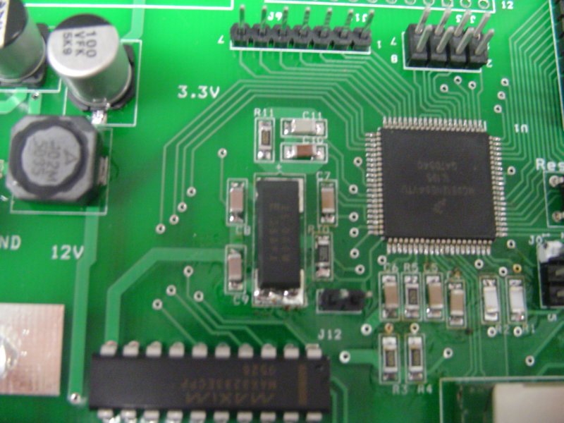
Here are the newest images of the PCB:
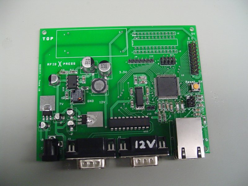 PCB - fully populated (top)
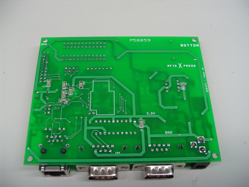 PCB - fully populated (bottom)
 PCB - oscillator circuitry
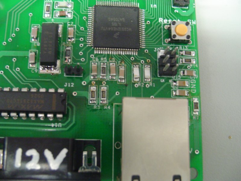 PCB - Ethernet circuitry
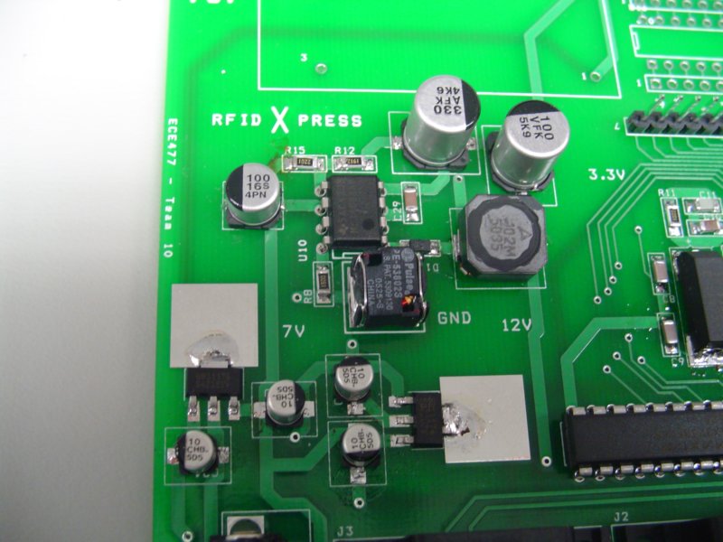 PCB - power supply
April 5, 2006 (1 hour):
Today we had a progress briefing in lab, and told Dr. Meyer that things
are going pretty well with the project right now. Chuck was able to provide us with a heat-dissipating copper
sheet to attach to our 7 - 3.3 V voltage regulator. Hopefully this will help reduce its operating temperature, as
we learned yesterday that it sinks considerably more current when we're actually running programs on the uC
(something we hadn't noticed when we did the 24-hour power supply burn-in).
Afterwards we attempted to load
some code to test the Ethernet circuit, but it was unsuccesful. I spent a while looking over datasheets and
discovered that at least a few of our pins (including Tx and Rx) on the schematic did not agree with the
Ethernet circuitry in the 9S12NE64 datasheet. Then I had to leave for another meeting, so Josh and Jared took
over. See their lab notebook entries for the solution they developed to the problem, which successfully
enabled us to ping the board by the end of the day.
April 6, 2006 (3 hours):
Tonight Jared and I worked on developing our main code for the program. It was
adapted largely off of the pseudocode that I developed a few weeks ago,
except this time we implemented our I.F.D.P.S.M. (Interrupt Flag Driven Polling State Machine) concept. We
finished most of the state transitions this evening, and have only the CANCEL_SESSION, PRINT, EMAIL,
SESSION_END, and FINISH_SESSION states remaining.
April 7, 2006 (1.5 hours):
Tonight Jared and I finished up the state transitions for the main program
and began including code functions that we have already written during the prototyping phase, such as
HandleRFID() and PollKeypad(). In both cases, modifications had to be made to the original functions. In
HandleRFID(), we removed the functionality that compared a serial number with a local list of serial numbers and
returned a customer name associated with that number, since this will now be handled in QueryDB(). Also, in
PollKeypad(), we removed the functionality that compared the keys entered with a stored PIN, since that is now
handled directly in the main function during the CAPTURE_PIN state.
Also, we decided to modify the way that we
handle PINs... we had originally used an int, and multiplied each digit entered by the appropriate power of 10 to
get a final 4-digit PIN. However, we realized that this would be difficult to deal with if the user pressed the
CLEAR button during PIN entry, meaning he/she wanted to remove the most recent digit. So, we have chosen to
store PINs as arrays of 4 characters.
Main Code and RFID/Keypad functions, v1.0
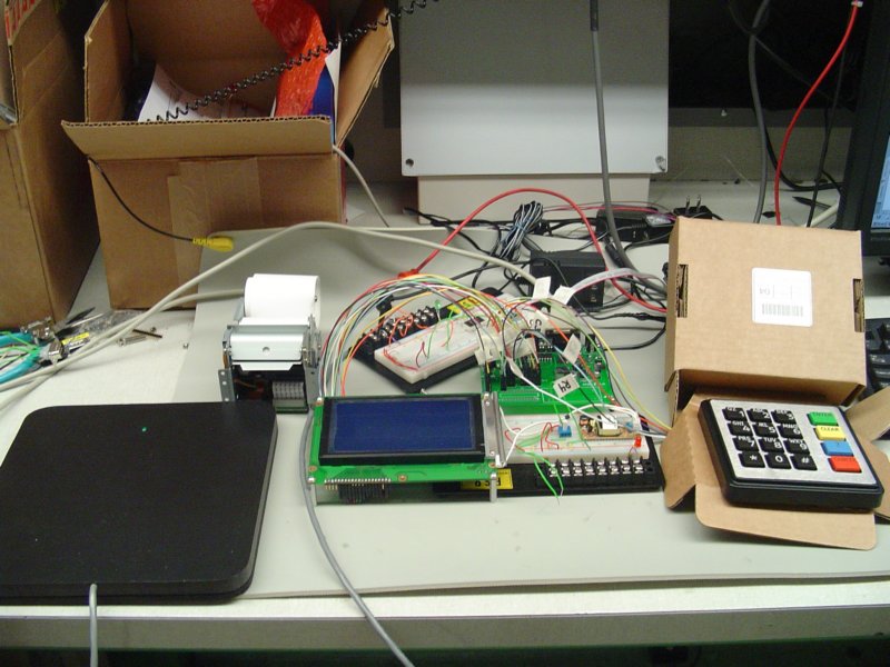
April 8, 2006 (2 hours):
Today in lab, I designed an output diagram for Jonathan's UpdateLCD() function
that utilized the states assigned in main() to determine what to display to the LCD. I came up with the general
organization of the shopping cart and gave him a state-by-state listing of what needed to be displayed. Jared and
I also began building a larger scale prototype system on the eval board, including the RFID reader, keypad, and
printer, to test the functionality of the main code and RFID and keypad functions we completed yesterday. We're
still working on debugging the compile errors, so hopefully I'll have some completed code to display tomorrow.
April 9, 2006 (6 hours):
Today was a long but successful day in lab. Jared and I continued to debug
the main code, and tried to implement interrupts with the RFID reader on the SCI1 port. However, as of right now,
we haven't been able to get them to work. The interrupt bit on the CCR register is set, we have set the
RDRF and RIE bits in SCI1_CR2, and the interrupt vector table properly points to the RFID interrupt handler.
Yet, neither the eval board nor our uC is able to properly detect an interrupt.
Jared came up with a way to simulate the interrupt just by polling the SCI1 data port each time through the
main loop (just now for debugging purposes). Hopefully we can get some help from Brian or Nick on Monday and
figure out what we're missing. Our eval board is also not properly communicating through either SCI port, which is
odd. We have resorted now to doing most of our debugging on our actual uC, since it is working beautifully.
Since Jonathan had completed UpdateLCD(), we ran it on the demo kit. I helped Jonathan and Jared debug
some errors that he had, especially with the formatting of the shopping cart screen. Afterwards, we were able
to get it working pretty well, as you can see below.
I also wrote the code for the PrintReceipt()
function today (bottom of main program). It built off of the
RFID/printer code that we developed earlier, as well as the data structure
organization that Jonathan determined with UpdateLCD(). The data structure specifies how our queries of the
database will return the user and item information. I tested the code with the printer and made this really
cool receipt!
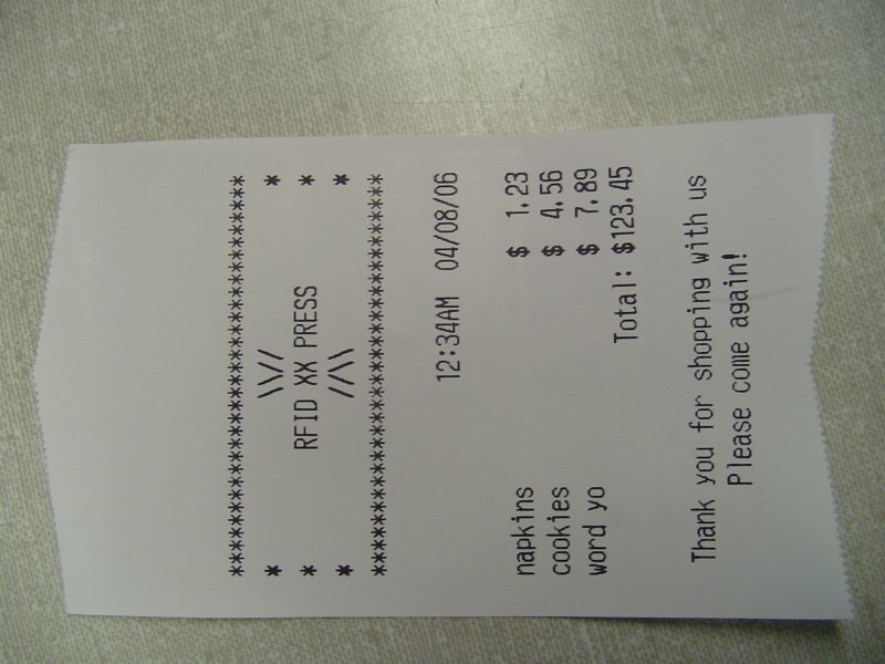 Receipt!
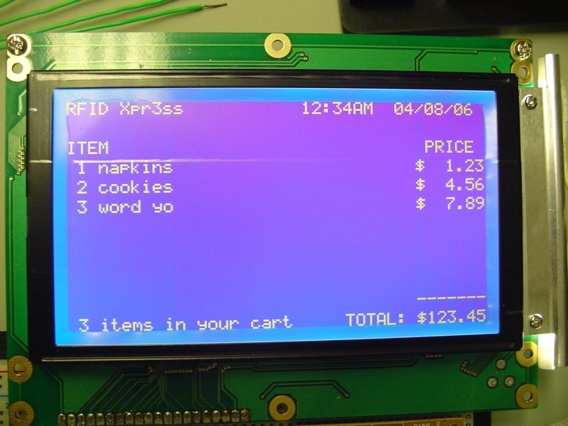 LCD shopping cart
WEEK 13 SUMMARY
Accomplishments: Completed board population (excluding LCD), developed main, RFID, keypad, and printer
functions.
Weekly Work Total: 19 hours
Project Work Total: 131 hours
Week 14
April 10, 2006 (2 hours):
Today Jared and I spent more time today trying to get SCI interrupts to work
for the RFID reader, and we were finally successful. We were suspicious of the CCR "I" bit from the beginning,
since we couldn't get ANY interrupts to work, not just the SCI. We thought that it made logical sense that
interrupts were enabled if the "I" bit was set. We tried to de-assert the "I" bit just in case, and it worked.
April 11, 2006 (2 hours):
With the RFID interrupts finally working and Jonathan having made some
special header-to-header cables, we decided to attach the keypad to our board and debug it. We have had to
relocate the 8 keypad wires (4 row wires, 4 column wires) to a different location on our PCB than was originally
planned because we learned after PCB submission that the ATD port cannot be used as output, and then we further
learned that although it can be used for digital input, it does not have a pull device register, and hence will
not allow the rows to be read correctly. The debugging of the keypad didn't go very well since we are getting
strange results - the enter key doesn't register ever, and the "3" key registers as the enter key. More debugging
to come soon, I guess.
I also spent some time making modifications to Jonathan's UpdateLCD() to fix some minor problems with
wording and the display overall. We think that the LCD code is generally complete except that I would like
to work on making a non-trivial function (if time permits) to calculate the length of dynamic fields,
such as the user name and item name, so that when they are displayed to the LCD, they are properly centered
and visually appealing.
April 11, 2006 (3.5 hours):
Tonight the team met to begin preparing for the TCSP tomorrow that focuses
on the FMECA worksheet for HW11. Josh and Jonathan worked on the powerpoint while Jared and I calculated
lambda_p and MTTF values, as well as determined possible failure modes for the design.
TCSP - Reliability and Safety Analysis
April 12, 2006 (3 hours):
After the TCSP this morning, Jared, Josh, and I went to the lab to try to
figure out why the keypad was still not working. Initially, all they keys were being registered properly by
polling the keypad at the end of the main loop, with the exception of the "3" key and the "Enter" key. We
determined, as I said earlier, that the error could not be with hardware because the other 2 columns and 3 rows
worked perfectly. Therefore, we reexamined our logic in the code structure to try to find a fault. We made
many different iterations of modifying the code - using RTI interrupts to poll the keypad, switching rows and
columns on the headers, removing the keypad from our board and prototyping it again on a breadboard to ensure
the proper key presses were actually sending out asserted signals. At one point, the keypad wires had been
attached to Port T, Port S, Port G, and Port H of our uC, and none of them solved the problem.
Jared thought that maye we were dealing with a race condition where the columns weren't being asserted
fast enough on the keypad before we checked if the rows were asserted. We finally had an idea to change the
location within the code where we increment the pollCounter variable
and perform the column strobing. The pollCounter variable is used to keep track of which column is asserted as we
poll the rows to see if any of them are asserted - by knowing the intersection, we can determine exactly which key
was pressed. After moving the column strobbing into the timer interrupt and setting a flag to poll in the main
loop, as you can see in this copy of the main code here, the key presses
on ALL the keys were working properly!
April 13, 2006 (4 hours):
I spent this evening completing the Homework 11 paper - Reliability and Safety
Analysis. I also edited Jared's paper once he completed it.
Homework 11 - Reliability and Safety Analysis
Homework 12 - Ethical and Environmental Impact Analysis
April 15, 2006 (3 hours):
Today in lab Jonathan and I worked on writing code for the Java server app to
maintain a copy of the shopping cart on the server side. I wrote the
MakeReceiptBody() function
that structured the email message to be sent to the server. I also helped Jared to connect the RFID reader,
printer, keypad, and LCD to all of the proper locations on our board, and we began the task of modifying all of our
test code to use the correct port pins for our board. We weren't able to finish tonight, but we'll work on it more
tomorrow.
April 16, 2006 (3 hours):
Today was a monumental day in lab! We completed our integration of all the
peripherals and made many changes to the ports and register settings in the code. We powered up our board to
start testing the states of the main loop. We found that the LCD was not initializing properly because the
reset never flashed and the startup screen wasn't displayed. While Jonathan worked on rectifying that problem,
Jared and I continued to debug the circuit without the visual aid of the LCD and found that the RFID interrupts
were being received correctly and the board was sending accurate user and item packets to the server. It was
also returning the proper matches with user or item information. The keypad was also being polled correctly.
Jonathan was working with some of the wires on the LCD and found that some of the connections were not good, so
he re-crimped the ribbon cables he made while Jared and I had to leave.
When Jared and I got back, Jonathan had left but the LCD was functioning! We ran the main code again
on the board and were very pleased with the results. It properly registered a key fob, identified the user and
prompted for the PIN, correctly identified an incorrect or correct pin, began a "shopping session", identified
RFID tags on items and properly received item data from the server, correctly handled a "cancel" or "clear" request
from the keypad, and registered an "enter" keypress to end the shopping session. We had to make several minor
changes to the code - one to fix the spacing on the shopping cart on the LCD since we had changed our field
length for the item name from 30 to 25, one to adjust the spacing of the total, another to fix an integer overflow
we were experiencing when calculating and displaying the total of the shopping cart to the LCD, and yet another to
properly adjust the total when the user removes an item from the shopping cart. The only things that didn't work
were that it didn't send an email receipt (because we were not connected to the Ethernet at the time) and it didn't
print a receipt. Jared and I were confused because we have tested the printer numerous times and know that it
works, even on our board. However, this time we used an actual gender changer to connect the two male connectors
together, which was the first time (we had made a gender changer on our own for debugging), and we think that
it is possible that the female-female gender changer switches the Tx and Rx pins. This could be causing our
printer problems. Next week we'll probably have to make another proprietary cable for the priner too!
We are elated to have most of the project functioning! Some changes that we anticipate making in the next
few days are changing the LCD to only show the hours and minutes (so that it doesn't refresh every second), adding
in a "default" state to the main loop to prevent it from going into a "zombie state," and working on the RFID
interrupts to minimize the number of "item not recognized" messages we receive and prevent the user from
scanning one item more than once.
Check out the main() function and the
UDP client app here.
Also take a look at the test circuit setup and recent PCB images:
 PCB with Keypad and LCD Wires Connected
 Test Circuit with Breadboards
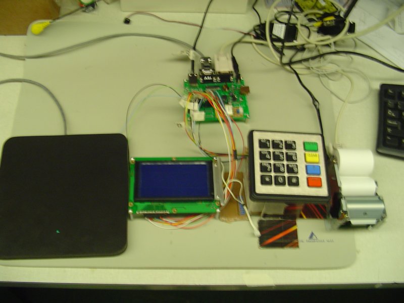 Test Circuit with Breadboards Removed
WEEK 14 SUMMARY
Accomplishments: Successfully implemented SCI interrupts, debugged keypad logic on our uC, completed
HW11 and HW12, modified LCD code to properly display messages, completed Ethernet code, debugged
packet sending, wired entire board, got complete board up and executing main code properly.
Weekly Work Total: 20.5 hours
Project Work Total: 151.5 hours
Week 15
April 18, 2006 (2 hours):
This afternoon in lab Jared and I continued to debug the entire circuit. We
hooked the board up to the Ethernet and emails sent successfully. However, the printer still wasn't working. We
looked at datasheets for the gender changer and used the DMM to find that it was wired straight through, so the
Tx and Rx pins weren't switched as we had thought. We then figured that the problem might be due to a lack of
current on the new power supply for the printer, as we used the 7 V supply that came with it to power the entire
board since it had a higher amperage. But when we moved the printer back onto the demo kit with the new power supply,
it worked fine. We then realized that we had never actually printed from our board with the printer because we had
only just recently bought the new power supply for it, so the problem might be with the SCI0 port. We changed all the
printer code over to operate on the SCI1 port, but it still didn't work. We then changed all the RFID receiver code
over to operate on the SCI0 port to see if it was functional at all, and it worked. I was skeptical of the RS-232 level
translator chip but had to leave for class.
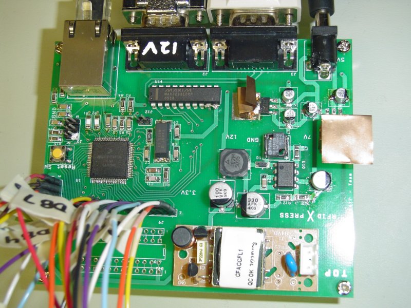
When I returned, Jared found that the error was actually in the schematic - we had wired an active low FORCEOFF pin
on the chip to ground when it was supposed to be wired to +3.3 V. This was disabling the SCI transmission entirely. After
cutting the pin and wiring it high, the printer functioned properly.
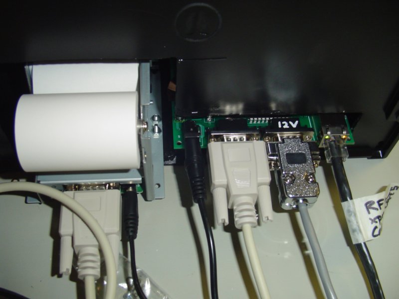
This image helps explain the fix that we made:
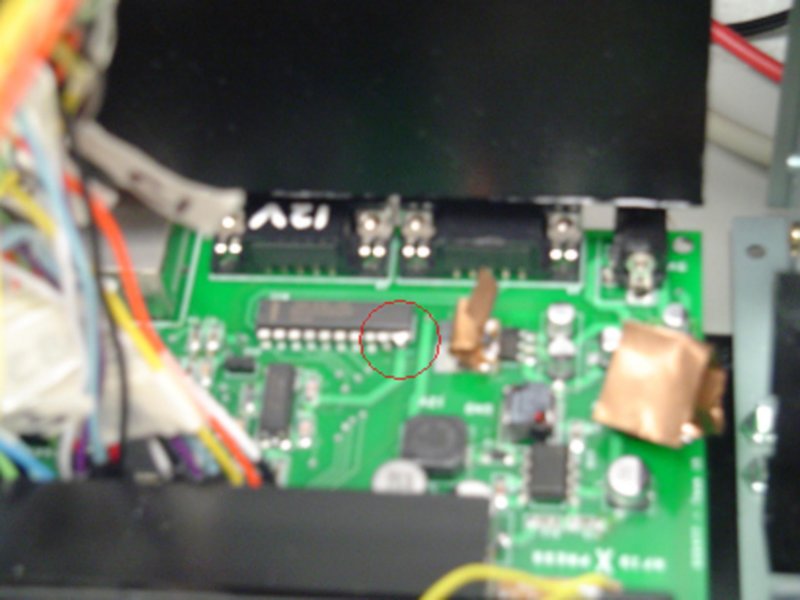 RSS232 Level Tranlator Fix
April 19, 2006 (3 hours):
Today we had our last progress briefing with Dr. Meyer, and we were able to tell him that
the project (or at least the PSSCs) were entirely functional. Chuck was able to get us copper tape to solder to the 5.0 V
regulator to help dissipate heat from the LCD backlight. Jared and I worked on fixing more bugs in the design, such as adding
comments to the database which differentiate between items and users so that a user cannot "purchase themselves" by swiping
his/her keyfob during a session (previously, the user's name, email, and PIN had been printed to the shopping cart on the LCD).
We found and corrected a bug in the print receipt function that incorrectly printed a '1' as the 1's digit of every total (I had
hardcoded a total of "$1111.11" at the start of the function for space holders and never actually overwrote the last character with
the real total). I also worked through the code adding comments and formatting it to be documentation-ready.
We were ready to tape our PSSC videos when we had a major problem with our circuit operation. After cleaning up our station
for the video, we reorganized the circuit and moved everything (keypad, LCD, RFID reader, printer, board) closer together so it
could all get in the shot. Then, the RFIDs stopped generating interrupts and the keypad began to function erratically.
We determined that the range of the reader had decreased tremendously and was only rarely detecting tags. We think that this
was due to some type of interference from the other components in the design. Luckily this won't be a problem because the
reader is separate from the station and attached via a 3 foot cable. We believe the keypad problems were a result of faulty
connections on the ribbon cables, so we are considering soldering at least one end of the ribbon cable to decrease the possibility
of error (though this would pose a problem if it ever needed to be replaced in the future).
Click here for the most recent copy of our main and supporting functions.
April 20, 2006 (4 hours):
Today in lab we videotaped our 5 PSSCs separately using Chuck's video camera
after he helped us fix problems with the tape. We also got our aluminum faceplate back from the machine shop after
they milled a hole for the LCD and an "X" for our logo. Jared and I drilled the holes for the LCD mounting.
Later in the day, Josh brought in the rest of the packaging, spray painted black. When we put all the
components inside, however, the keypad began acting erratically. On the LCD, we could see that the keypad was
registering keypresses automatically for the user's PIN and could not authenticate the user. We realized that
the back of the keypad, when touched by hand, would register keypresses (since the backing is made of metal). We
found a rubber material that came with the keypad, which we attached to the back of it to try to shield the keypad
from the aluminum. We didn't think that alulminum should be conducting or holding a charge, but somehow, that's
what seemed to be occurring. After mounting the keypad with the rubber shielding, it still was registering
automatic incorrect keypresses. We discovered that the aluminum face probably needed to be grounded, so we
soldered on some additional headers to the PCB where the headers for our GAL22V10 would have been (now unused)
and flywired a ground signal and power signal to them (the extra GND and PWRs will be used for blue LEDs
that will be mounted inside the packaging to illuminate the "X" in the logo). After attaching a ground terminal
to one of the screws on the aluminum faceplate, everything worked perfectly. The RFID receiver was now properly
shielded from the other system components as well.
Here are some of the newest final images of the system:
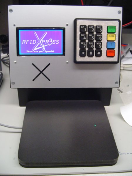 Packaging - Front View #1
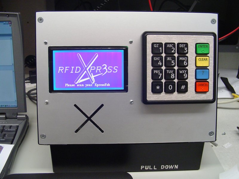 Packaging - Front View #2
 Packaging - Rear View
April 21, 2006 (2 hours):
In lab today we taped our PSSCs again, this time in one continuous video
and inside our final packaging (the previous videos were taken before the packaging was complete). Nick also
demo'd our project to ensure that we satisfied all of our PSSCs. Then Jared and I went to Radio Shack to
buy the blue LEDs for the logo and the plexiglass sheet to protect the logo and LCD.
April 23, 2006 (4 hours):
Today I completed the
Senior Design Report and posted it on the website for the rest
of the team to read over.
WEEK 15 SUMMARY
Accomplishments: Identified and fixed problem with SCI0 printer transmission, debugged LCD display and
server communications, completed assembly of project packaging, videotaped PSSC demonstration,
demonstrated PSSCs to Nick, completed Senior Design Report.
Weekly Work Total: 15 hours
Project Work Total: 166.5 hours
Week 16
April 25, 2006 (2 hours):
This afternoon I got started on the User Manual document, mainly working
on the marketing-style introduction and establishing a skeleton file for the rest of the report.
April 27, 2006 (4 hours):
Jared and I went to Radio Shack today to purchase more blue LEDs of
higher intensity. We mounted them inside the case by flywiring resistors between the LED leads and the
unused header positions for the GAL22V10. We also printed some decals for the case that included our logo and team
name. It looks really neat and professional now.
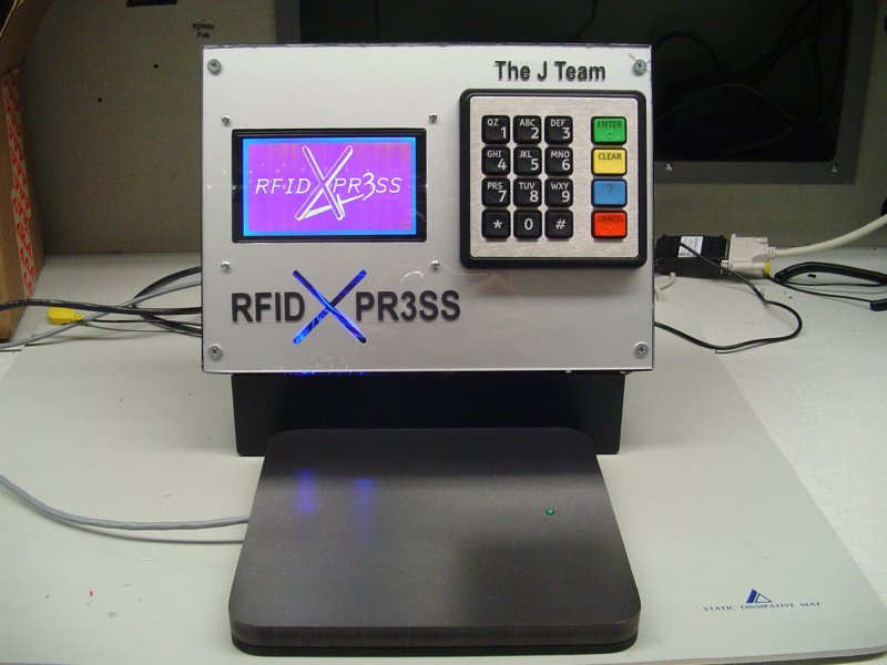 Final Packaging - Front View #1
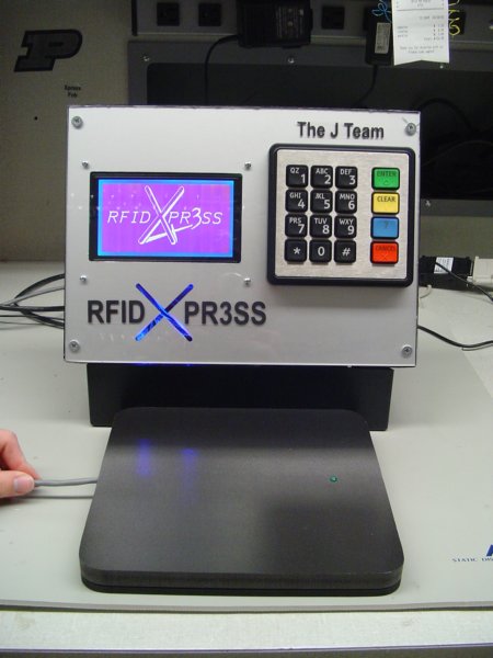 Final Packaging - Front View #2
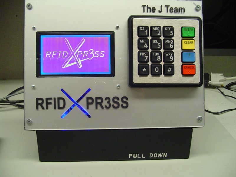 Final Packaging - Front View #3
April 27, 2006 (2 hours):
Jared and I worked together to organize the
Bonus Presentation for ECE270 for tomorrow. Most of the information
was already written in the summary report or in a previous TCSP, so it wasn't too difficult to compile.
April 28, 2006 (3 hours):
Tonight Jared helped me finish the User Manual.
At times it was difficult to write because we wrote it from the perspective of a commercially available product,
which would have somewhat different setup instructions than our prototype system currently does (i.e., populating
the database automatically vs. typing the serial numbers and products in by hand, etc.). We posted it on the site
for Jonathan and Josh to review.
April 29, 2006 (4 hours):
I spent this evening making revisions to my HW5 (Schematic & Theory of
Operation) and HW11 (Safety & Reliability Analysis) assignments and adding them to the final report. Much of
the schematic paper had to be altered due to changes in the port assignments that we were forced to make during
development (such as the relocation of the LCD wiring from the ATD ports which could only be used for input, which
thereby displaced the keypad assignments). Once the report is fully completed, it will be uploaded to the
website.
April 30, 2006 (12 hours):
Jared and I spent this entire day revising and editing the final report.
There were many updates that needed to be made to particular papers, especially the design considerations
and software narrative. I also completed the Version 2 Changes and the Summary and Conclusions sections of the
final report.
Click below to view the final product:
Final Report
WEEK 16 SUMMARY
Accomplishments: Completed exterior design of packaging, delivered PSSC videos in class, delivered
bonus presentation to ECE270 students, completed User Manual and individual sections
of final report.
Weekly Work Total: 27 hours
Project Work Total: 193.5 hours