Research advances large-scale nanoshaping of ultrasmooth 3D crystalline metallic structures Latest results chronicled in Dec. 12 issue of Science
Research advances large-scale nanoshaping of ultrasmooth 3D crystalline metallic structures
background-position: 100% 15%;
background-size: 100% !important;
}
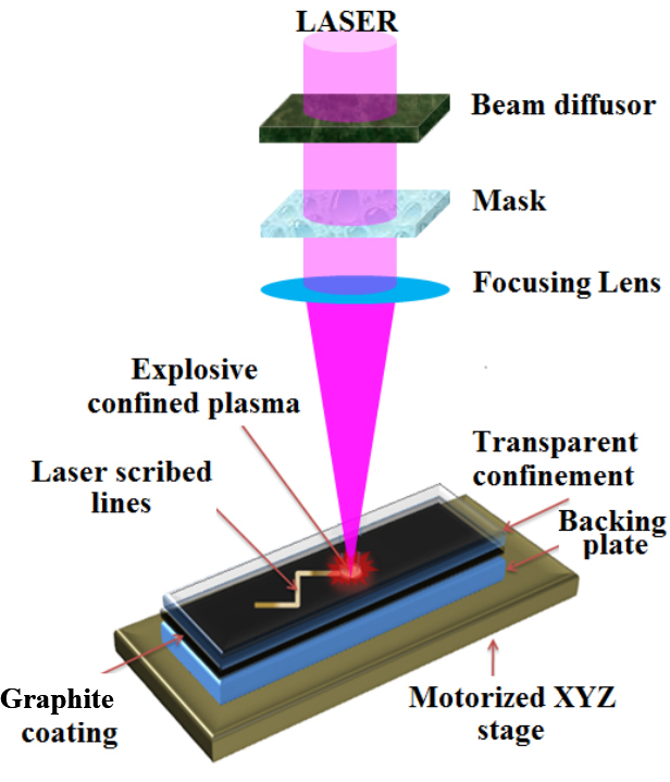
Research led by Gary Cheng, associate professor of industrial engineering, is breaking new ground in nanomanufacturing. Central to his work is the use of a pulsing laser to induce a shockwave inside a multilayered film topped with a glass sheet. In the latest results, researchers showed how to create large patterns of three-dimensional nanoshapes from metal sheets. The concept represents a potential manufacturing approach to inexpensive mass production of plasmonic metamaterials for advanced technologies.
“Traditionally it has been really difficult to deform a crystalline material into a nanomold because at these small sizes materials are super-hard,” Cheng says. Whereas other researchers have created nanoshapes out of relatively soft materials, the new work shows how to create shapes out of hard metals. “These nanoshapes have extremely smooth surfaces, which is potentially very advantageous for commercial applications,” Cheng says. Moreover, the new method, called laser shock-induced shaping, creates shapes out of crystalline metals, potentially giving them ideal mechanical and optical properties using a bench-top system capable of mass producing the shapes inexpensively.
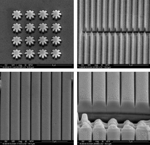
To overcome the limitation of formability at nanoscale, this transformative approach realizes a high strain rate deformation in nanoscale. The multilayered sandwich structure has a nanomold at the bottom. Exposing this layered film to a pulsing laser causes the ablative layers to generate an ionized gas and a shockwave that exerts a downward pressure, forcing the metal film into the mold. The 3D crystalline metallic structures, some as small as 10 nanometers, include pyramids, gears, bars, grooves and a fishnet pattern stamped out of titanium, aluminum, copper, gold and silver.
Think of it as a mini-explosion that’s contained so that the force is directed downward,” says research collaborator Minghao Qi, associate professor of electrical and computer engineering. A key benefit of the shock-induced forming is sharp corners, or high-fidelity structures, and aspect ratios as high as 5.

“It is a very challenging task from a fabrication point of view to create ultra-smooth, high-fidelity nanostructures,” Qi says. “Normally, when metals recrystallize they form grains and that makes them more or less rough. Previous tries to form metal nanostructures have had to resort to some sort of amorphous metal, which gives them smooth surfaces and high strength, but they also have drawbacks including very high resistance. For potential applications in nanoelectronics, optoelectronics and plasmonics you want properties such as low resistance and thermal conductivity, and you want it to be very smooth. You also want it to be very high fidelity in terms of the pattern, sharp corners, vertical sidewalls, and those are very difficult to create. Before Gary's breakthrough, I thought it unlikely to achieve all of the good qualities together.”
Hybrid structures could expand applications
The researchers also created hybrid structures that combine metal with graphene, an ultrathin sheet of carbon that is promising for various technologies. Such hybrid structures could enhance plasmonic effects and bring metamaterial perfect absorbers, or MPAs, which have potential applications in optoelectronics and wireless communications. Plasmonic metamaterials could harness clouds of electrons called surface plasmons to manipulate and control light. They have engineered surfaces that contain features, patterns or elements on the scale of nanometers that enable unprecedented control of light and could bring advances such as high-speed electronics, advanced sensors and solar cells.
The research had its early beginnings between Cheng and his graduate students five years ago.
While silicon is too brittle to be considered practical for roll-to-roll nanomanufacturing, the discovery does lay the groundwork for future work to create molds out of more ductile and durable materials such as metals. “If you want to stamp 3D metal molds, you need to have a stamp first, and if you want a smooth metal surface you need to make your stamps very smooth, almost atomically smooth in silicon,” Qi says.
The nanosecond-pulsing laser is critical to the process. “When you make it fast, the materials have a higher formability,” Cheng says. While the pressure generated is not high — less than 2 gigapascals — the strain rate applied at the corners of the molds is considerably greater, resulting in high-fidelity nanostructures. The research team spent two years studying and documenting the effect with a variety of measurement techniques. "And we did a lot of molecular dynamics simulations to study what happens during this high strain rate,” he says.
Qi’s group created the silicon molds using facilities in Purdue’s Birck Nanotechnology Center. “Super high-fidelity metallic structures could make possible new devices based on patterned metals, roll-to-roll manufacturing of nanostructures and even large-scale metallic structures with functionalized surfaces, perhaps for aircraft,” Cheng says, “but such potential applications are likely far in the future.” Analyses showed the structures — such as the tiny pyramidal shape with a 500 nm base — are made of a single crystal.
The Science paper was authored by Purdue doctoral students Huang Gao, Yaowu Hu, Ji Li and Yingling Yang; researcher Ramses V. Martinez from Harvard; Purdue research assistant professor Yi Xuan, Purdue research associate Chunyu Li; UCSD professor Jian Luo; Purdue associate professor Minghao Qi; and Cheng. Future research may focus on using the technique to create a roll-to-roll manufacturing system, which is used in many industries including paper and sheet-metal production.
The research is ongoing and supported by National Science Foundation (grants CMMI–0547636, CMMI–1436305, CMMI–1120577 and CNS–1126688), National Institutes of Health (grant 1R01RR026273-01), Defense Threat Reduction Agency (grant HDTRA1-10-1-0106) and Office of Naval Research (grant N00014-11-1-0678). Other support has come from a Senior Research Associateship award by the National Research Council, the FP7 People program under the project Marie Curie IOF–275148 and an NSSEFF fellowship (N00014-15-1-0030).
In other research
In related work, Cheng’s group has shown how to create synthetic nanodiamond films and patterns from graphite, with potential applications ranging from biosensors to computer chips. “The biggest advantage is that you can selectively deposit nanodiamond on rigid surfaces without the high temperatures and pressures normally needed to produce synthetic diamond,” he says. “We do this at room temperature and without a high temperature and pressure chamber, so this process could significantly lower the cost of making diamond. In addition, we realize a direct writing technique that could selectively write nanodiamond in designed patterns.” The researchers have named the process confined pulse laser deposition (CPLD).
The ability to selectively “write” lines of diamond on surfaces could be practical for various potential applications including biosensors, quantum computing, fuel cells and next-generation computer chips. The technique works by using a multilayered film that includes a layer of graphite topped with a glass cover sheet. Exposing this layered structure to an ultrafast-pulsing laser instantly converts the graphite to anionized plasma and creates a downward pressure. The graphite plasma then quickly solidifies into diamond. The glass sheet confines the plasma to keep it from escaping, allowing it to form a nanodiamond coating.
“These are super-small diamonds and the coating is super-strong, so it could be used for high-temperature sensors,” Cheng says. Findings were detailed in a paper that appeared online in the Nature journal Scientific Reports. The paper was authored by former Purdue doctoral students Yuefeng Wang, Yingling Yang, Ji Li and Martin Y. Zhang; postdoctoral research associate Jiayi Shao; doctoral students Qiong Nian and Liang Tang; and Cheng.
“This technique has several important advantages to allow scalable processing, such as high speed, direct writing without a catalyst, selective and flexible processing, low cost without expensive pico/femtosecond laser systems and high temperature/vacuum chambers,” Cheng says.
The research team confirmed that the structures are diamonds using a variety of techniques including transmission electron microscopy, X-ray diffraction and the measurement of electrical resistance. A U.S. patent application has been filed on the concept through the Purdue Office of Technology Commercialization. More research is needed to commercialize the technique.