Formation of Potential Wells and Barriers in Semiconductor Heterostructures and their Utilization
The figure above shows a sequence that indicates the consequences of the atomic scale abrupt stacking of dissimilar semiconductor materials. The misalignment of electron bands creates new barriers and wells as a superstructure extending over many atomic layers. The new quantum wells for new quantum states that extend over many atomic layers. These states have similar transitions to the original atomic states.
The new, man-made states can be designed for devices that have tuned transitions for photon absorption (detectors), photon emission (lasers, LEDs), and electron tunneling (fast logic, memory)

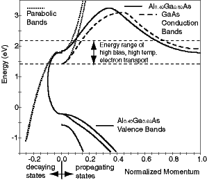
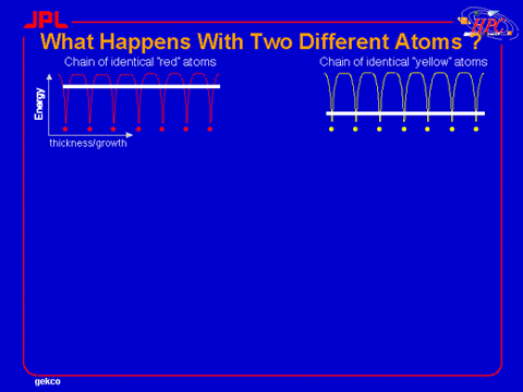
Electron bands are formed due to the regular ordering of atoms in semiconductor crystal. Within a band the electrons are allowed to move "freely" throughout the whole crystal. The concepts can be grasped in such simplified single band models. However, quantitative modeling of electron transport through heterostructures requires a more detailed understanding of the bandstructure physics.