Example Quantum Dot (QD) Implementations
The Challenge: The smaller the better:
The technological challenge for electronic QD applications is to create structures in which the electron addition energy (E) is significantly larger than the thermal energy (kT). If the electron addition energy is large compared to the thermal energy, an external (controlled) energy needs to be provided to inject an electron into the QD. This energy is quantized and the effect is called Coulomb blockade. The observation of Coulomb blockade in a variety of systems has been subject to intense research in the last few years. The general recipe is to make the QDs as small as possible to increase the quantization energy (delta E) and the charging energy (U).
Metallic QDs:
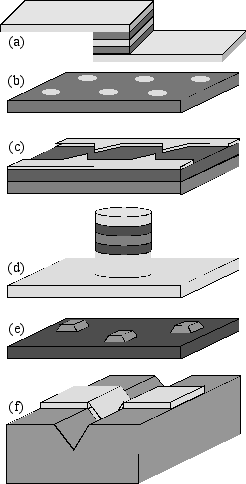
The figure provides sketches of the typical QD structures that have been explored. The earliest QDs were proposed and built in metal systems where metallic layers were separated by thin oxides and the lateral features were determined by lithography. In these systems the electron number in a dot is large (Fig. a). These structures are limited by the available lithography technology. Since the dots were relatively large, the electron addition energy is small and the operation of the devices has been limited to 1K or less.
Recent experiments have extracted small (10-50 nm) metal clusters out of chemical suspensions (Fig. b). Such small metal clusters have a chance to be operated at room temperatures, however the processes are not integrated with any other semiconductor technology. The technique is sometimes described as self-assembled and self-organized since no lithographic technique is involved in the size and placement of these QDs.
Horizontal QDs:
Electron waveguides can be patterned with split-gate technology to confine a 2-D electron puddle (Fig. c). Also these structures are limited by current lithography techniques that limits their operation temperature to typically less than 1K. Recently horizontal QDs were produced with scanning tunneling microscope (STM) and shown to exhibit Coulomb blockade at room temperature. However, STM lithography does not lend itself to mass production (see notes on lithography below).
Vertical QDs:
Mesa etching of resonant tunneling diodes with small mesa sizes results in so-called vertical QDs (Fig. d). Natural surface depletion reduces the available "space" for electrons further. These QDs have the potential to be operated at room temperature. The technological problem with these dots is the creation of surface states at the side walls due to the reactive ion etching.
Pyramidal or Dome Shaped QDs:
Growth of a material with a different lattice constant than the substrate can result in natural clustering of that material. These QDs are subject to significant stress and strain and tend to grow in a pyramidal or dome shaped form (Fig e). This type of QD is characterized as self-assembled or self-organized as well. These QDs can be made small enough to exhibit their quantum mechanical characteristics at room temperature. These are the kind of QDs that are used to replace the 1-D confinement quantum wells in quantum well lasers and photodetectors for JPL missions.
Trench QDs:
Yet another method to generate atomically small structures without the limitation of present lithography technology is use of non-isotropic etching techniques. Depending on the orientation of the crystal, deep, triangular wedges can be etched into semiconductors. At the apex an electron waveguide forms that can be depleted to become a QD (Fig. 2).
New Lithography:
New approaches to push lithography to atomic limits are being investigated as well. Scanning tunneling microscopes (STM) have been shown to be able to write atomically fine lines to generate horizontal QDs. The approaches however do not provide an entry into any kind of mass production of QD arrays although devices with parallel STM tips are developed. Standard optical lithography cannot lead to pattern dimensions needed for QDs. Electron beam lithography can write sufficiently fine lines (i.e. vertical QDs), however it is slow. Efforts to speed up the electron beam writing process by use of parallel micro-columns are under way. Another lithography technique based on a pattern imprint has recently been demonstrated. It is, however, not beyond the first experimental phases.
Figure Caption: Various quantum dot implementations. (a) metal and metal oxide systems patterned by lithography. (b) metallic dots out of chemical suspensions. (c) lateral quantum dots through electrical gating of heterostructures. (d) vertical quantum dots through wet etching of quantum well structures. (e) pyramidal quantum dots through self-assembled growth. (f) trench quantum wire.