Matthias Tan

PROJECT OVERVIEW: Atomistic Modeling of Metallic Conduction Limits in Quasi 1-D Silicon Nanowires

INTRODUCTION:

  • Experiments observed tunability between metallic and insulating behavior in ultra-thin, highly-doped Si:P nanowires
  • Charge carrier localization induced by random doping fluctuations likely cause of metallic conduction limits

METHODOLOGY:

  • Large-scale atomistic modeling (NEMO)
  • Self-consistent TB simulations of bandstructure / density of states (DOS)

RESULTS:

  • Successfully modeled disordered nanowires up to 10nm in length
  • Observation of DOS energy gap for 10nm wire shows trend towards carrier localization
  • Published in PRL 113, 246802, 2014, B. Weber, H. Ryu, Y.-H. M. Tan, et.al.

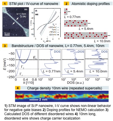
Powerpoint slide as pdf.