Home
> Research Group
> Members
> Amritanshu Palaria
> Overview (surface and strain effects in nanostructures)
Overview (surface and strain effects in nanostructures)
| Overview (surface and strain effects in nanostructures) | Amritanshu Palaria, Alejandro Strachan, Gerhard Klimeck |
|
Methods employed/ developed: density functional theory, reactive force-field molecular dynamics, modified tight binding |
|
|
Structure and Properties of ~1 nm diameter silicon nanowires
|
|
|
Electrical properties of Si-Ge-Si bars
|
|
|
Adaptive tight binding
|
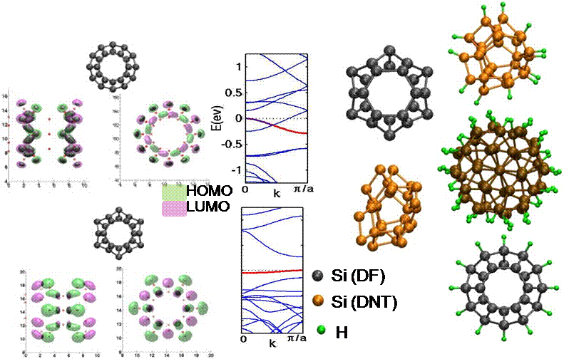
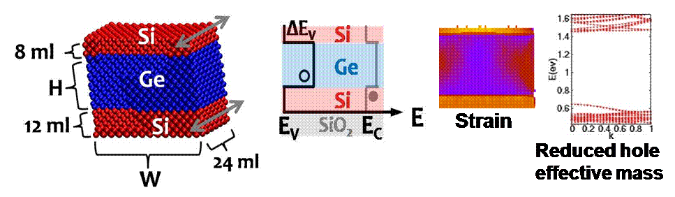

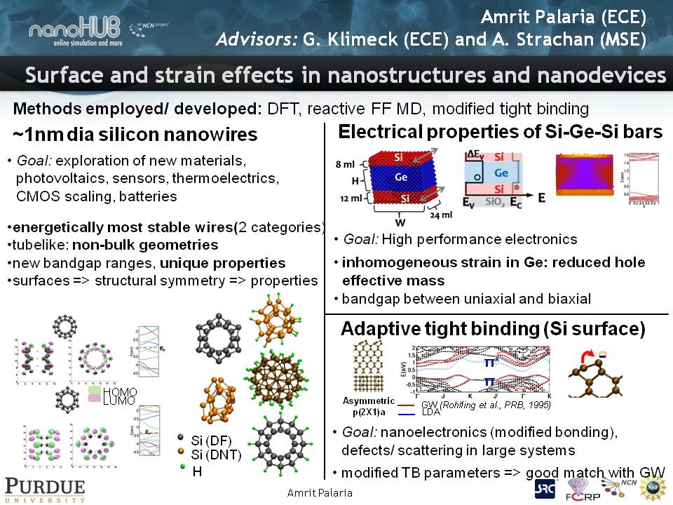
Powerpoint slide as pdf or as image below.