Andy Robison's Lab Notebook
Week 01
January 14 (2 hours):
Met as a team after class to discuss preliminary project proposal.
January 15, 2010 (1 hours):
Met as a team to discuss design implementation and assign different
components to research.
WEEK 01 SUMMARY
Accomplishments: Submitted preliminary project proposal.
Weekly Work Total: 3 hours
Project Work Total: 3 hours
Week 02
January 20, 2010 (4 hours):
Met
as a team to formulate PSSC for presentation in class. The team also
solidified part requirements and packaging ideas, which included the
design of custom clear keys and the use of an LCD monitor under the
keys to change the key characters.
January 21, 2010 (3 hours):
Met as a team to finish the final project proposal. Researched ways to
implement VGA, Unicode, and a touch screen in the design.
WEEK 02 SUMMARY
Accomplishments: PSSC and project proposal finalized.
Weekly Work Total: 7 hours
Project Work Total: 10 hours
Week 03
January 24, 2010 (2 hours):
Browsed the internet for a touchscreen solution. Settled on the LCD-010,
which is designed for electronic projects and has sample code for a
range of microcontrollers listed on the Gravitech page.
January 27, 2010 (1 hours):
Met
as a team to discuss what parts we would select for our major
components and what interface standard we would use for the computer
interface.
January 28, 2010 (3 hours):
Met
as a team to discuss design requirements. Discussed options for
microcontrollers and determined what information still needed to be
researched before a final microcontroller selection could be made.
Divided the parts among group members to be researched. Objective of
research was to determine the number of pins required for each
component and electrical characteristics.
January 30, 2010 (3 hours):
Found electrical
schematic for LCD and datasheets for the LCD and onboard graphics
controller, touch screen controller, and octal bus transceivers.
Determined that the LCD requires a +5V supply, but all onboard chips
are +3.3V.
Datasheets:
1. LCD Schematic
2. Graphics
Controller
3. Touch Controller
4. Octal Bus Transceiver
5. Summary of Pins
WEEK 03 SUMMARY
Accomplishments: Design constraints set for selecting components.
Weekly Work Total: 9 hours
Project Work Total: 19 hours
Week 04
January 31, 2010 (2 hours):
Met as a group to discuss our individual findings for components. Selected
a microcontroller and FPGA for generating VGA output to the LCD screen
that will display the characters under the screen.
Chose the following components:
Microchip PIC32MX575F512L microcontroller
Altera Cyclone II FPGA
3M SD card reader
Atmel Flash IC chip
The PIC microcontroller was chosen because it has 3 SPI ports, which
will be needed to read the touch coordinates from the touch screen, as
well as interface with the SD card reader, and Flash chip.
February 4, 2010 (3 hours):
Met
as a group to complete HW3: Design Constraints Analysis.
WEEK 04 SUMMARY
Accomplishments: Completed the Design Constraint Analysis and
chose the major components for the project.
Weekly Work Total: 5 hours
Project Work Total: 24 hours
Week 05
February 9, 2010 (2 hours):
Met as a group to prepare for TCSP 3 and begin HW4. Created a 3D CAD
drawing that would give a fairly accurate representation of the
position of each component within the overall package. Then we
made a preliminary layout for the keyboard PCB and the motherboard PCB.
February 10, 2010 (3 hours):
Met as a group before class to complete TCSP 3.
Met
as a group again later to create a parts list and order the major
project components. During the TCSP presentation, David suggested
using a daisy chain of shift registers to read the entire keyboard
layout at once instead of using the PLD design. This requires an
additional SPI interface to connect the keyboard to the
microcontroller, so a different microcontroller was chosen from the
same PIC family, which has 4 SPI ports.
Chosen microcontroller:
Microchip PIC32MX695F512L
February 11, 2010 (6 hours):
Talked with Chuck after class about how to create the keys for the
keyboard. He was confident that we could find pushbuttons/switches
small enough to fit under each key. He also suggested that I check the
board manufacturer's web site to see what all they offer in the $33
Each package, which is the one that we will be using in the course.
Unfortunately, they do not do any cutouts or tabs on the boards, so the
slots that the transparent keys are mounted over will have to be cut in
house, which Chuck says is not a big deal. We just have to remember to
draw the slot outline on the PCB's solder mask and keep traces as far
from the cutout edges as possible.
I downloaded the demo version of PADS and completed the first 2 of 4
tutorials on the website.
Met as a team later to complete HW4.
WEEK 05 SUMMARY
Accomplishments: Ordered parts, chose more appropriate microcontroller, and created CAD drawings of the package and PCB designs.
Weekly Work Total: 11 hours
Project Work Total: 35 hours
Week 06
February 14, 2010 (7 hours):
Continued working through the PADS tutorials, including the
microcontroller tutorial.
Met as a group to begin HW5: Theory of Operation and Hardware Design
Narrative. We created a much more detailed layout of the keyboard PCB
with the footprints for the shift registers instead of the PLDs used
previously. We also researched and chose resistor packs and very small
push buttons to be used to implement the key-press circuits.
The following two pushbutton options were discussed:
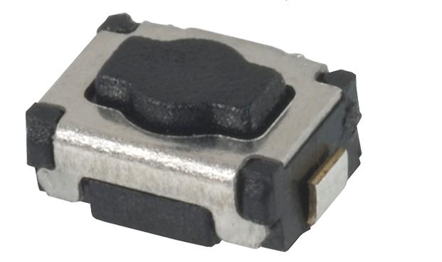
TL1015BF160QG
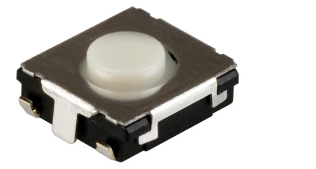
EVQ-Q2B02W
The pushbuttons were chosen for their small footprints, which is a
requirement to fit all of the pushbuttons on our keyboard PCB with
enough room to spare for signal traces for each one.

10 K 15 resistor pack
The resistor packs were chosen to save space on the PCB rather than
place individual resistors for each signal trace on the board.
February 15, 2010 (5 hours):
Today I
finished the PADS tutorials in preparation for creating the schematics
for the keyboard and mainboard PCBs. I then began searching
through the microcontroller documentation for pinouts. I needed
to determine which pins were for general purpose I/O (GPIO) as well as
determine which pins were used for the SPI ports, since our design
requires all 4 SPI interfaces. The pin-out diagram for out
microcontroller package documents which peripherals and ports each of
the pins is mapped to.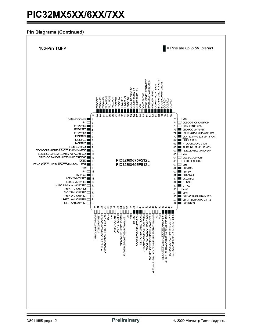
I assigned the SPI ports to all of the peripherals first, and then I
assigned all of the pins on Port E to the touch screen graphics data
port for simplicity. The rest of the connections are control
signals that were assigned to GPIO in a configuration that I felt would
be easiest for PCB layout.
February 16, 2010 (4 hours):
The microcontroller has several sets of power and ground pins, which
each need bypass capacitors placed placed across them. Section 2
of the microcontroller documentation has a recommended layout which I
duplicated in our schematic. CEFC is used to stabalize the
internal regulator and was recommended to be 10uF in the Electrical
Specifications section of the documentation.

I also searched through the documentation for the pins which will be
required for programming and debugging. The PIC32 has both ICSP
and JTAG pins for programming and debugging the microcontroller.
It was recommended that they all have 50ohm resistors in series for ESD
protection.
I created a PCB footprint and schematic symbol in my PADS library for
the microcontroller. I labeled the function of each pin in the
schematic as it pertains to our design instead of labeling every
function that each pin is capable of, as in the pin-out diagram in the
documentation.
February 17, 2010 (5 hours):
Finished the first draft of the microcontroller schematic for the TCSP
presentation. I created a sheet for the microcontroller in PADS
with off page connectors to the other peripherals to make the schematic
easier to read.
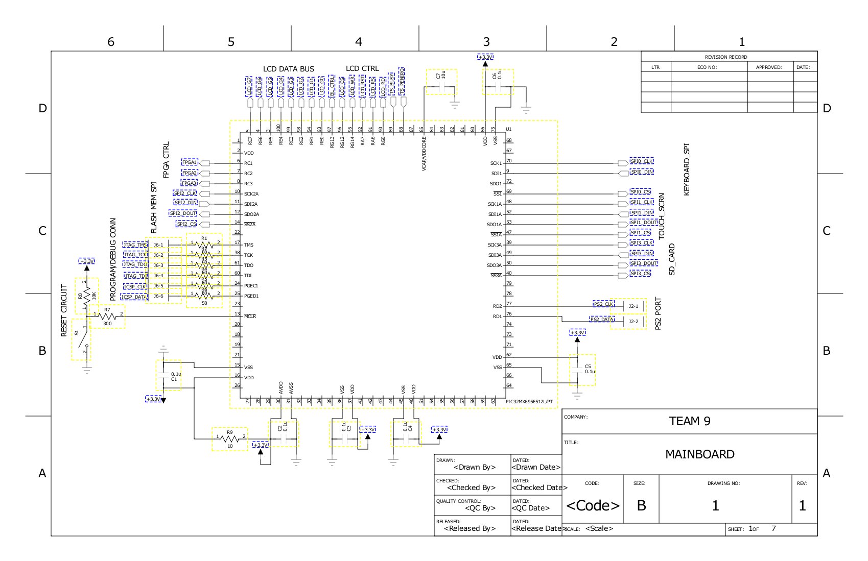
I consulted with Luke about how the FPGA would be implemented and what
connections would need to be made to the FPGA, both to the
microcontroller and the flash memory. To make the connections to
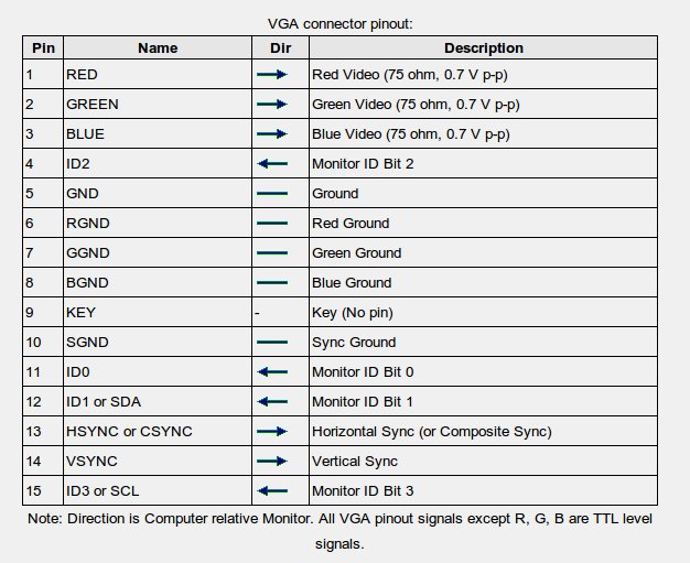
the VGA connector, I found a chart online with the VGA pinout and a
brief description of each pin's function.
I continued to create schematic symbols in my PADS library for the other major design components on the mainboard.
February 18, 2010 (5 hours):
Today I finished the mainboard schematic except for the power supply
circuit and keyboard, which are being drawn up by Dhruv. Using
PADS, the power and ground nets from the power supply circuit will
automatically be connected to the rest of the design once the power
supply sheet is added.
The first draft, which was submitted for homework 5 can be found here.
I found a website for the SD card pin-outs and used the following diagram for our schematic:

February 19, 2010 (1 hour):
Today I looked over all of the schematics, including the Power and
Keyboard schematics drawn up by Dhruv to double check for mistakes
before submission. I then purchased the LCD-010 touch screen.
WEEK 06 SUMMARY
Accomplishments: This week, I searched through the
microcontroller documentation to find pin-outs, electrical
requirements, and programming pins. I then decided which pins
would need to be used in our design, such as the SPI ports, and
organized the connections for the easiest PCB layout. Once this
was done, I created schematic symbols and PCB footprints for all of the
major components and completed the first draft of the mainboard
schematic in PADS.
Weekly Work Total: 27 hours
Project Work Total: 62 hours
Week 07
February 21 (3 hours):
Dhruv and Luke
ordered several of the parts and sent me a BOM so that I could get PCB
footprint information for our specific parts. I then worked to
create PCB footprints and link them with the schematic file in PADS.

I manually created the SD card footprint from the datasheet.
February 22, 2010 (4 hours):
I spoke with
Dhruv and we decided it would be best if we divided the PCB work
between the two of us, so I will be designing the mainboard layout and
he will take the keyboard layout. I spoke with Chuck about which
headers we had available in lab for making connections to things off of
the board. He pointed out the 0.1" pin pitch headers in lab and
said that there are tools in lab for making connectors to mate with
them. It also happens that PADS has a generic footprint for
headers with this pitch already. I updated the schematic with
connectors for the keyboard and PS/2 and linked the connectors to these
PCB header footprints. I also added a schematic symbol and PCB
footprint to my PADS library for the SPI flash memory chip in the new
BOM, and added a sheet for the SPI flash to the mainboard schematic
file.
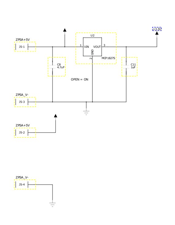
February 23, 2010 (10 hours):
I added the
power supply schematic as a new sheet in the PADS mainboard
schematic. PADS already had PCB footprints for the regulators,
and a 0.1" header will be used to connect to the AC/DC converter
card. I created a custom footprint for the current limiters,
which was just 2 plated through holes spaced according to the datasheet.
I noticed that the 3.3V regulator was only rated for 250mA, which may
not be adequate given all of the 3.3V parts. I placed all of the
footprints on a preliminary board layout for the TCSP and looked at
different layout possibilities to minimize trace length and reduce the
number of vias. The correct PCB footprint for the FPGA is
yet to be determined.
February 24, 2010 (12 hours):
I spoke with
Dhruv after the TCSP presentation and we decided that the voltage
regulators would be in drop-out since they were being supplied by
switching voltage supplies with exactly 3.3V and 5V outputs in the
current design. The voltage regulators need an input voltage that
is higher than the output voltage, so the 3.3V switching regulator will
be removed from the design and the 5V AC/DC converter will supply the
5V rail. This should be fine since the only 5V part is the touch
screen, and it has a 3.3V regulator on board. I added up the
power requirements for all of the parts we have so far, and found that
our current 3.3V regulator does not supply enough current to make me
feel comfortable with it. I found another 3.3V regulator from Microchip
which uses the 3 lead TO-220 package, which is a very standard package
and pin-out for voltage regulators, including some already in lab.
With these changes, I redrew the power supply schematic and linked the components to PCB footprints in PADS.
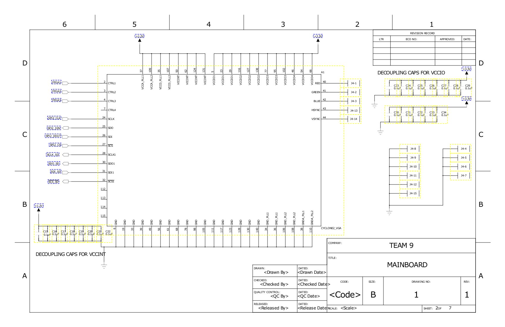
Luke determined exactly which FPGA package we will be needing for our design, and I found pinout descriptions
on the Altera website. I updated our schematic to reflect the
recommended capacitor placements and power requirements of the
FPGA. The core voltage of the FPGA is 1.2V, instead of 3.3V, so
another regulator was added to the power supply circuit. I also
changed the PCB footprint linked to the schematic for the FPGA.
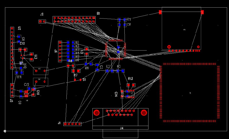
February 25, 2010 (11 hours):
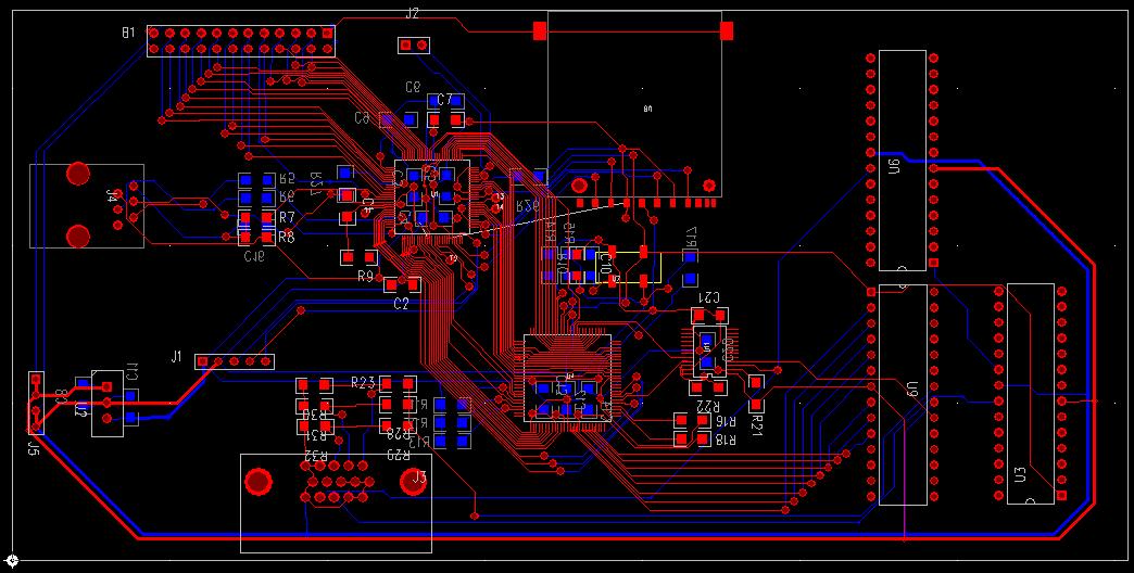
Today I created a new PCB layout, again taking trace length and the
number of vias into account. I used the 1206 package for all of the
capacitors and resistors, which is surface mount, and placed all of the
bypass capacitors on the bottom layer, underneath the supplied IC
whenever possible. For both the microcontroller and FPGA, the
capacitors were specified to be within 1/4" of the power and ground
pins. The FPGA was very difficult to fit all of the capacitors next to
and run all of the traces to the power and ground pins, especially
since there are two power nets on the FPGA. Once all of the bypass
capacitors were placed, I ran the power and ground traces first, with
an effort to minimize the size of current loops on the board since
these would create noise in the data lines. I also avoided making
right angles whenever possible, which could create manufacturing
problems. For the sake of time, and because I know more design changes
are coming, I autorouted the rest of the traces. This will be
inadequate for the final design, since the autorouter does not make
very smart decisions when it comes to the previously mentioned
considerations.
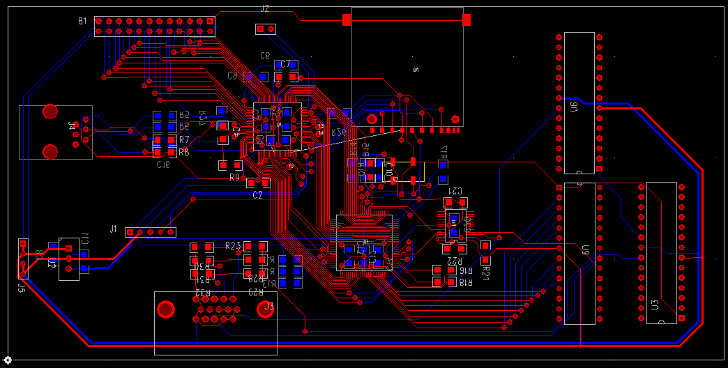
Version 1 of the
Schematic
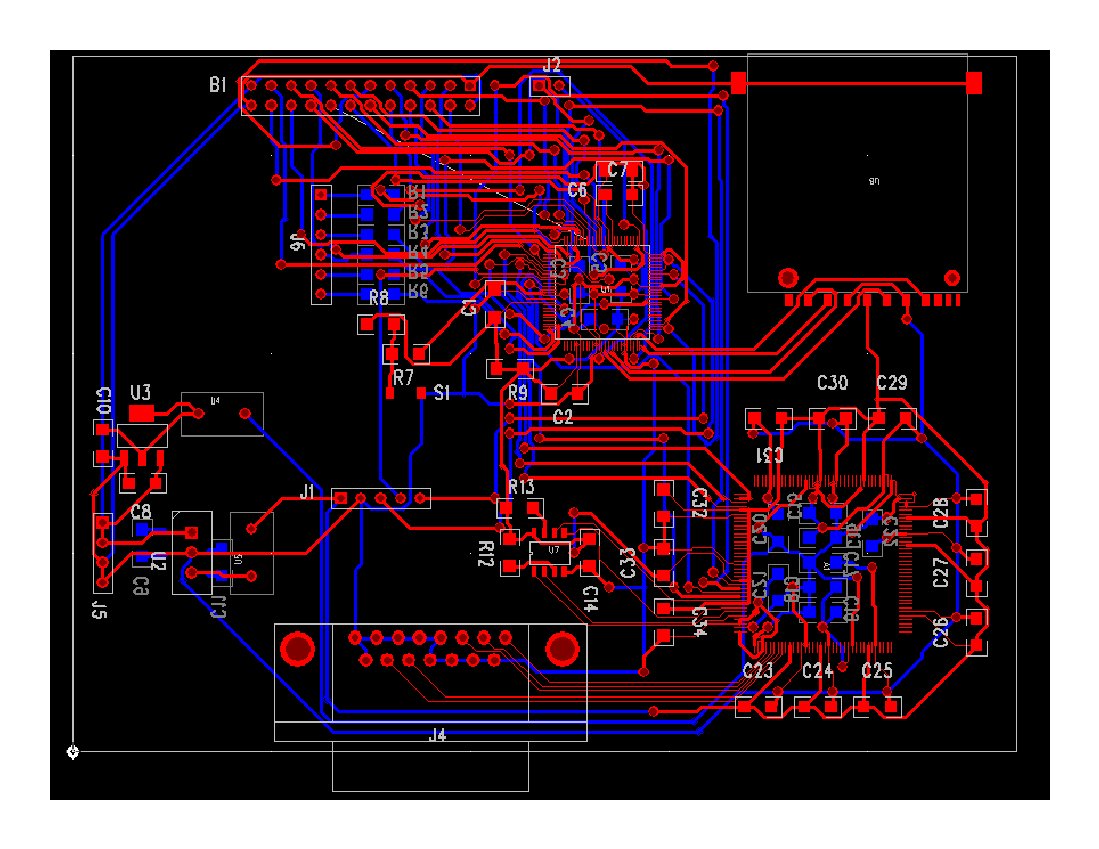
Version 1 of the PCB
WEEK 07 SUMMARY
Accomplishments:
Weekly Work Total: 40 hours
Project Work Total: 102 hours
Week 08
March 2 (10 hours):
The FPGA is capable of doing much more than what we need it to do
(displaying a static VGA image). So, since the image we are displaying
is static and very simple, we will generate our own VGA signals and get
rid of the FPGA, since it would require another programmer, a 1.2V
power supply net, and quite a bit of real estate on the PCB to do a
very simple task. Luke and Ethan created a block diagram and a new
list of parts for the VGA circuit, which I used to update the schematic
and PCB footprints in my PADS library.

In addition to the components indicated in the block diagram, I added a
level
translator recommended by Chuck to interface the 3.3V logic of the
SRAM IC to the 5V logic of the PLDs, which will generate the sync
pulses.
The new schematic for the VGA circuit is as follows: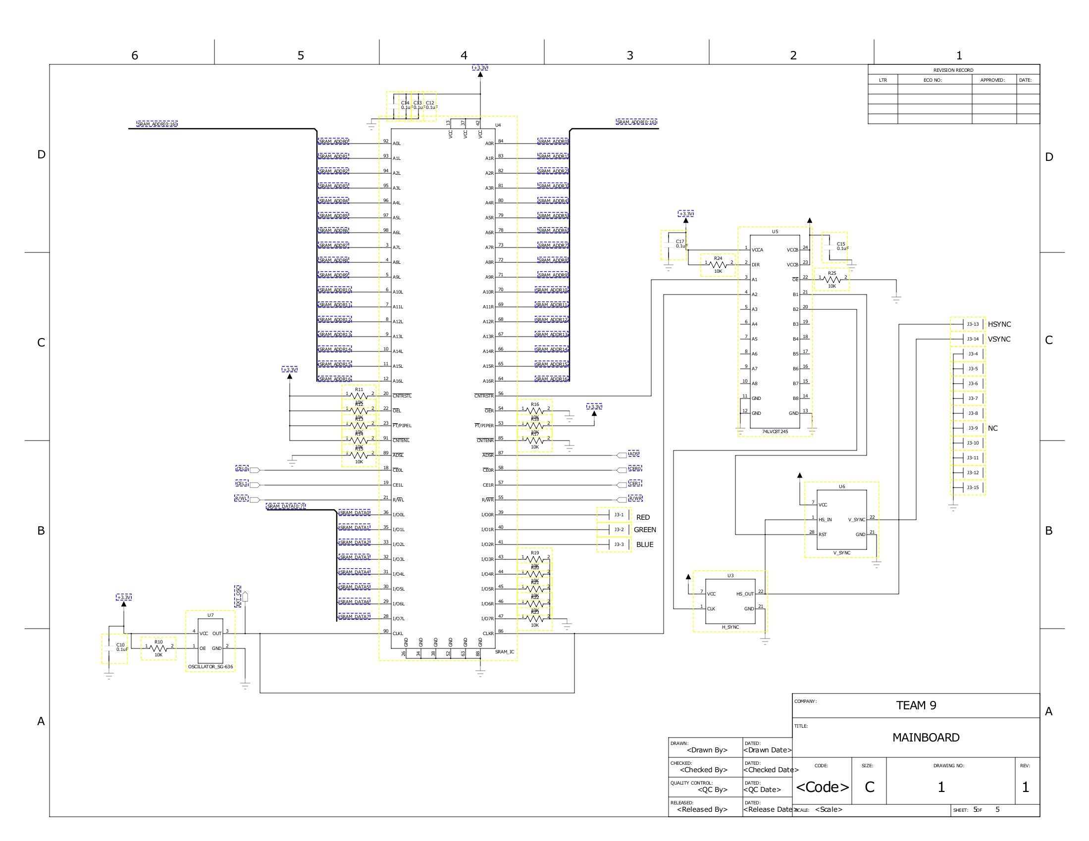
With the FPGA now removed from the design, the 1.2V regulator is no
longer necessary. The current limiters were also removed from the
power supply design since they weren't necessary, resulting in the
following design:
Once the schematic was updated, the new netlist was pushed to PADS
Layout, and a new PCB layout was created. Again, I manually rounted
the power and ground traces to ensure that current loops were
minimized, and manually connected the bypass capacitors to the
appropriate power and ground pins on all of the ICs. Once this was
done, I autorouted the rest of the traces since a few more
modifications to the VGA circuit are still being discussed.
Design Review Schematic

Design Review Mainboard
March 3 (3 hours):
We met as a team to finalize the design review presentation and play devil's advocate for each other.
WEEK 08 SUMMARY
Accomplishments: This week, a new VGA circuit was designed and
the schematic was updated to reflect the changes, removing the
FPGA. The new schematic symbols and PCB footprints for the new
parts in the VGA circuit were created in my PADS library. A new
PCB was created for this major design change, and after the power and
ground traces were routed, the rest of the traces were autorouted for
the Design Review.
Weekly Work Total: 13 hours
Project Work Total: 115 hours
Week 09
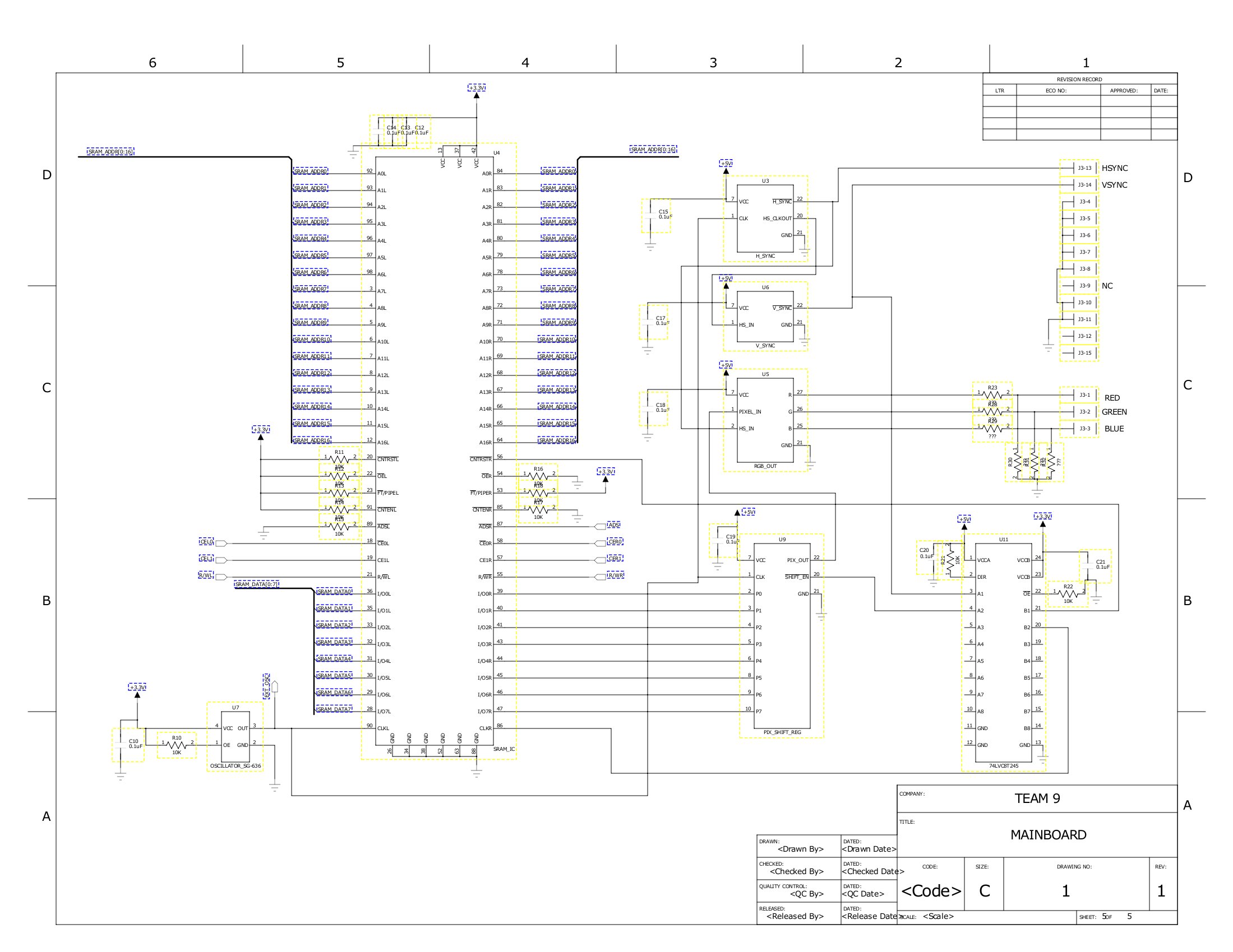
March 7 (8 hours):
Met in the lab to start
testing the VGA circuit, which was constructed using PLDs and an
oscillator on a bread board to drive the VGA monitor pins. The
PCB layout for the design review was very disorganized and routing all
of the traces with two 100 pin ICs on the board has become very
challenging. In an attempt to simplify the layout, I again looked
at the microcontroller pin-out diagram to rethink pin
assignments. The SRAM IC has a 17-bit address bus and an 8-bit
data bus, which connect to the microcontroller, so I reassigned the
microcontroller pins so that these traces could all be run between the
two ICs without needing to cross over each other at any point. I
did the same for as many control signals as possible from the
microcontroller.
March 8 (12 hours):
Continued to update the microcontroller pin assignments and make the changes to the mainboard schematic.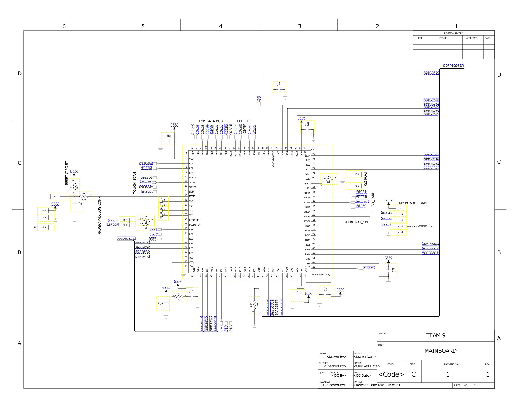
My teammates worked all night to get the VGA test circuit working so
far as to display an all white screen on the monitor. I discussed
the changes to the circuit with them, which included a new (3rd) PLD
for shifting the display bits out from the SRAM data bus to the VGA RGB
pins. Testing of the VGA circuit continued, but now the goal is
to create a bit pattern on the screen using DIP switches to simulate
the SRAM data bus. Once this is accomplished, the VGA circuit
schematic can be finalized.
March 9 (14 hours):
In the morning I met
with Luke to finalize the VGA schematic. The design we were using
yesterday worked once a few changes were made to the PLD timing.
 Resistor dividers were placed at the RGB pins of the VGA connector to
allow us to adjust the voltage swing in the final build. Sockets
will be used for the PLDs on the final board, but they will have the
same PCB footprint. We also updated the programming connector to match the connector used with the Microchip programmer.
With the schematic finalized, and the PCB footprints all positioned to
minimize trace length and vias, I made a 1:1 printout of the board to
ensure that all of the parts fit on their respective footprints with
ample room to solder. I then began to manually route every single
trace on the mainboard using PADS Router.
Resistor dividers were placed at the RGB pins of the VGA connector to
allow us to adjust the voltage swing in the final build. Sockets
will be used for the PLDs on the final board, but they will have the
same PCB footprint. We also updated the programming connector to match the connector used with the Microchip programmer.
With the schematic finalized, and the PCB footprints all positioned to
minimize trace length and vias, I made a 1:1 printout of the board to
ensure that all of the parts fit on their respective footprints with
ample room to solder. I then began to manually route every single
trace on the mainboard using PADS Router.
March 10 (5 hours):
Today, I added mounting
holes to the mainboard PCB and a fourth PLD to AND the RGB signals
together with the H-sync pulse. We then got the proof-of-parts
completed.
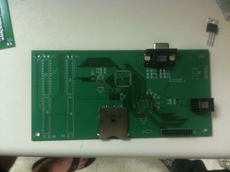
Final Schematic
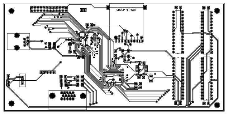 PCB Top Layer
PCB Bottom Layer
WEEK 09 SUMMARY
Accomplishments: This week the schematic was finalized once the
VGA circuit had been constructed and tested. I reassigned most of
the microcontroller pins to make trace routing more organized.
The PCB layout for the mainboard was then finalized and every trace was
manually routed. The mounting holes were added to the four
corners of the board and 1:1 printouts were made to ensure that all of
the parts fit on their respective footprints. Once this was done,
the proof-of-parts was completed, and we started the process of
ordering our printed circuit boards.
Weekly Work Total: 39 hours
Project Work Total: 154 hours
Week 10
WEEK 10 SUMMARY
Accomplishments: Spring Break. Got a tan from some natural sunlight instead of flourescent bulbs.
Weekly Work Total: 0 hours
Project Work Total: 154 hours
Week 11
WEEK 11 SUMMARY
Accomplishments:
Weekly Work Total: 0 hours
Project Work Total: 154 hours
Week 12
March 29 (2 hours):
Updated Homework 6 to reflect the latest design.
March 30 (1 hour):
We got our PCBs in today. Dhruv started soldering a few components to the mainboard.

March 31 (4 hours):
Dhruv and I soldered the
microcontroller and corresponding capacitors and resistors on the
mainboard. The ICD3 programmer identified the microcontroller
correctly and loaded a test program onto the microcontroller for the
first time.
April 1 (1 hour):
Checked the cable connections for the touch screen and connected it for testing with Ethan's code.
WEEK 12 SUMMARY
Accomplishments: This week all of my time devoted to the project
was spent soldering components to the PCBs, which we received at the
beginning of the week, and providing support for the people writing
software by answering questions related to the schematic. At this
point, nothing appears to be wrong with the schematic or PCB design, so
I have taken a slight step back from the project for the time being
while the software is written.
Weekly Work Total: 8 hours
Project Work Total: 164 hours
Week 13
April 7 (3 hours):
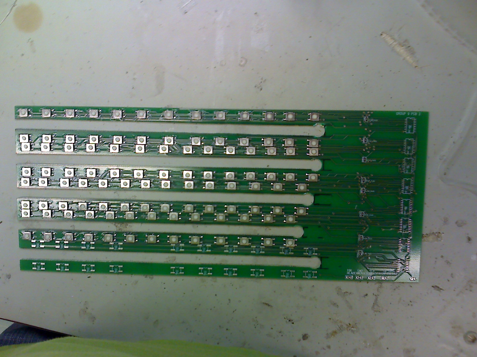
Dhruv and I handed our
keyboard PCB over to Chuck, so that he could cut the slots in it that
will go under the rows of keys. I then began soldering the
pushbuttons for the keyboard keys after Dhruv soldered the tiny
resistor packs on. I also pulled a PS/2 cable off of an old
keyboard and put a connector on the end of it to interface the clock
and data lines to our mainboard.
April 8 (1 hours):
I continued soldering the pushbuttons to the keyboard PCB.
April 9 (1 hours):
Still soldering the last of the pushbuttons to the keyboard PCB.
WEEK 13 SUMMARY
Accomplishments: This week we got the slots cut in the keyboard
PCB and soldered the pushbuttons to it for the keyboard keys. I
also put a PS/2 cable together for interfacing our mainboard to a
PC. The rest of the team worked on debugging the software.
Weekly Work Total: 5 hours
Project Work Total: 169 hours
Week 14
April 11 (3 hours):
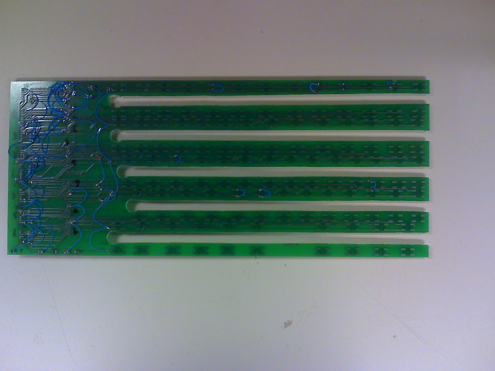
Dhruv finished soldering
the pushbuttons to the board along with the shift registers. I
began making a cable for the keyboard PCB and soldering the headers to
the board, but discovered that the bottom copper layer had been
replaced with the top layer when manufactured. Fortunately, the
bottom layer connections can be replaced by soldering wires to the vias.
I also helped Luke troubleshoot/test the new touch circuit for the Nintendo DS screen.
April 13 (2 hours):
The microcontroller
mysteriously stopped programming today, so Chuck had to remove it for
us. Dhruv soldered the spare microcontroller on, and the board
would not power up anymore. Dhruv and I discovered that there was
a short between the 3.3V power and ground rails on the board.
Using an idea from David to use the Agilent DMM in lab in 4-wire mode,
we checked the resistance between the power and ground rails at various
parts of the board. In 4-wire mode, the DMM can measure
resistance with micro-ohm accuracy, which allowed us to narrow the
location of the short down to an area near the microcontroller.
Under further inspection, Dhruv found a solder bridge as thin as a hair
between a power and ground pin on the microcontroller. After
removing that, operation returned to normal.
April 16 (9 hours):
Today I purchased two
different types of adhesive to test on the keyboard keys for
gluing the Plexiglas squares to the pushbuttons. One was
fast drying Krazy glue, and the other was Elmer's Stix-all cement,
which takes a full day to cure, but is designed to withstand
vibrations. I fasted two pushbuttons to a plastic square, one
with each type of adhesive and left it to cure over the weekend.

The blue mark represents the Elmer's cement.
I made a run to Lafayette Electronic to purchase some wiring and
connectors for the AC to DC power supply circuit. A panel mount
AC socket will be used to connect the case to the 110V wall outlet, and
then inside the case, a Y-splitter will connect the monitor and AC/DC
power supply to the 110VAC source.
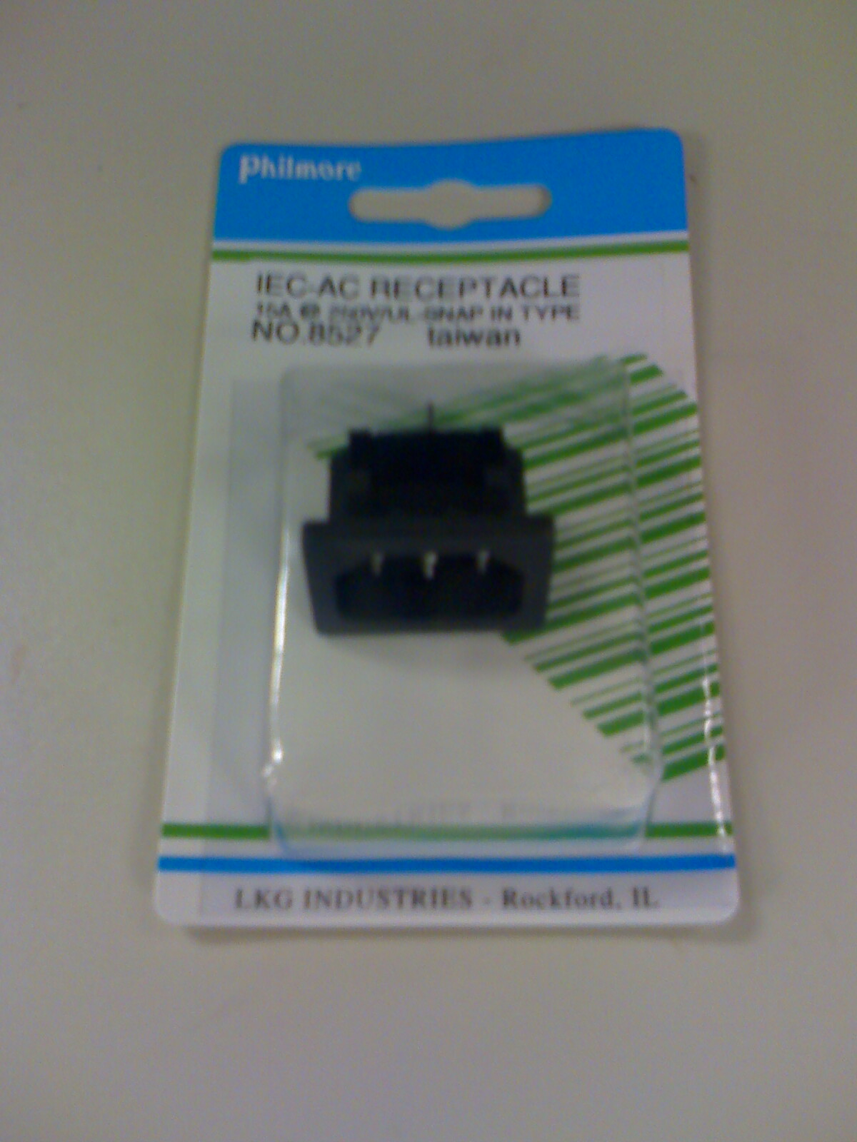
I also purchased a SPST
switch, which will be placed in the AC line wire to switch the 110VAC
source to both the monitor and AC/DC board on and off.

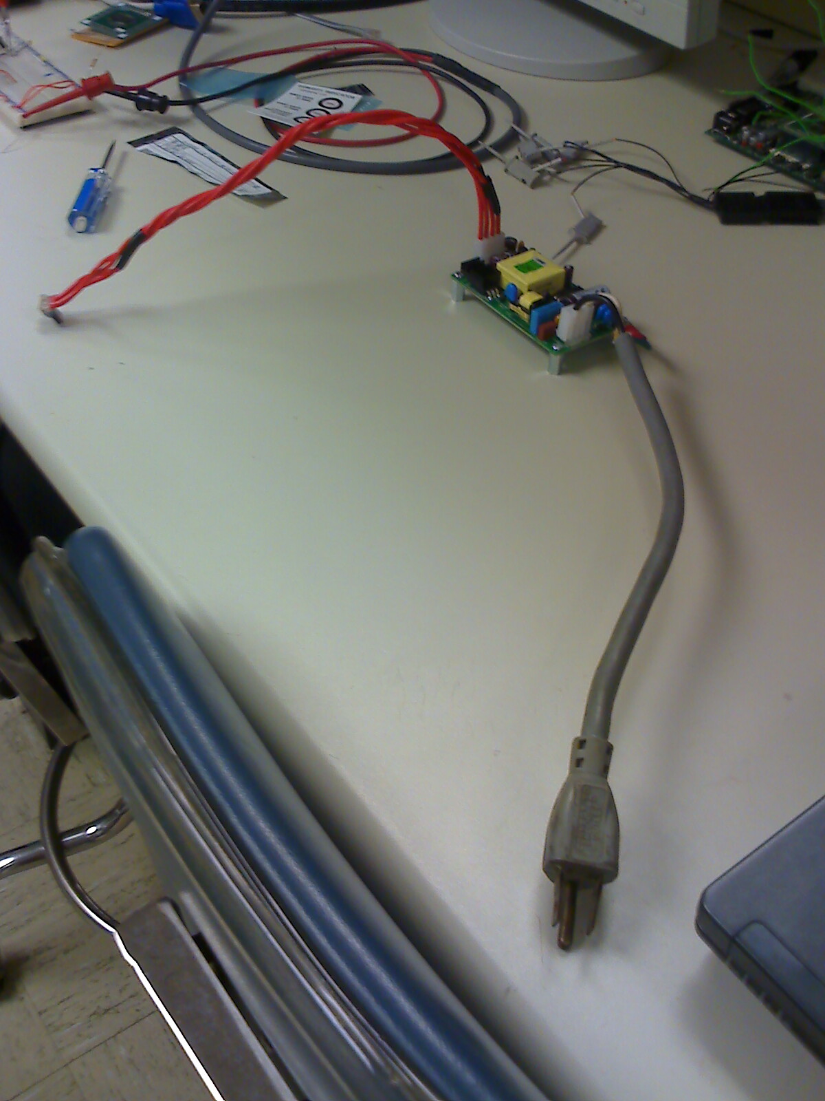
I then used 16 AWG wire to make a cable that will connect the AC/DC
power supply board to the main board, and cut the 3-prong AC plug off
of the end of a cable to attach it to the AC/DC power supply input.
After attaching the AC plug to the AC/DC power supply, I tested it to
ensure that 5V were being output. I then connected the supply to
the mainboard and successfully powered it using the AC/DC supply board.

I finished the day by continuing to flywire the keyboard PCB.
WEEK 14 SUMMARY
Accomplishments: This week, after discovering the mistake on the
keyboard PCB, we began flywiring to all of the vias to recreate the
bottom layer connections. We also got a touch screen solution
working using a Nintendo DS touch screen and comparators. After
the microcontroller stopped working, we soldered a new one in place and
got the mainboard fully functional again after removing a solder bridge.
Weekly Work Total: 14 hours
Project Work Total: 183 hours
Week 15
April 21 (6 hours):
Dhruv and I finally
finished flywiring the Keyboard PCB. I made a cable to connect
the Keyboard PCB to the Mainboard PCB using a color code for each
connection while Dhruv checked some nets on the keyboard for
continutity.
Keyboard Cable Color Code:
Power --> red
Ground --> black
Clock --> yellow
Data --> white
Parallel/Serial Select --> purple
Dhruv found that the clock signal did not have continuity to all of the
shift registers, and after examining the flywire connections, we found
that one was missing. After this fix, the board connections all
seemed to be OK.
Luke and Ethan wrote a program that would read the status of the board
and then serially transmit the databits back out. By monitoring
the clock and data output signals on the oscilloscope, we were able to
verify the keyboard functionality by pressing each key one by one and
watching the data bits change on the output in real time.

April 22 (2 hours):
I decided that the best option for a faceplate for the HULK would be a
rigid piece of plastic. This would be easier to make cutouts in,
and it would not pose a danger of shorting connections on the Keyboard
PCB. I spoke to Meyer Plastics in Lafayette, and they recommended
a type of PVC board and agreed to cut an 18"x18" piece for us out of
their stock. Ethan and I laid the components in the aluminum case
that we will be using and measured all of the appropriate dimensions
for cutouts in the case and faceplate.


WEEK 15 SUMMARY
Accomplishments: This week, the flywiring was completed and the
connections on the keyboard PCB were all checked to ensure that the
flywiring had been done correctly. The keyboard functionality was
then checked by writing a program that would read the state of the
keyboard and then write the data bits back on the data output
pin. The data output and clock were monitored using an
oscilloscope. The packaging design was finalized and the rest of
the materials for packaging the project were acquired.
Weekly Work Total: 8 hours
Project Work Total: 191 hours
Week 16
April 25 (8 hours):
The code for the PS/2 connection and the keyboard are both working
separately on the development board, and Luke is working to combine the
code to allow us to type on the keyboard and transmit the data to a
computer. The code for the touchscreen is also working by itself, but
could be combined with the others to allow us to change the language
being transmitted for a demonstration in the near future. In order to
do this, I first needed to construct the circuit that will interface
the Nintendo DS touch screen with our mainboard via comparators. The
touch screen is a resistive film, so using our setup, we will connect
the Y-axis pins to power and ground and one of the X-axis pins will
output a voltage dependent on where along the Y-axis the screen is
touched. Thus, using 3 comparators, each set to transition to a high
output at different input voltage levels determined by voltage
dividers, the screen can be divided into three separtate regions, and
the microcontroller will be able to tell which region is being pressed
by the outputs of the three comparators.
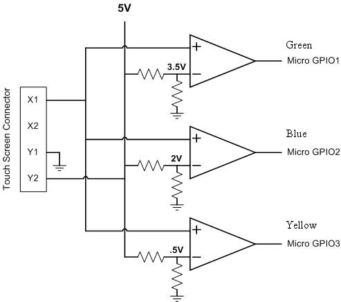
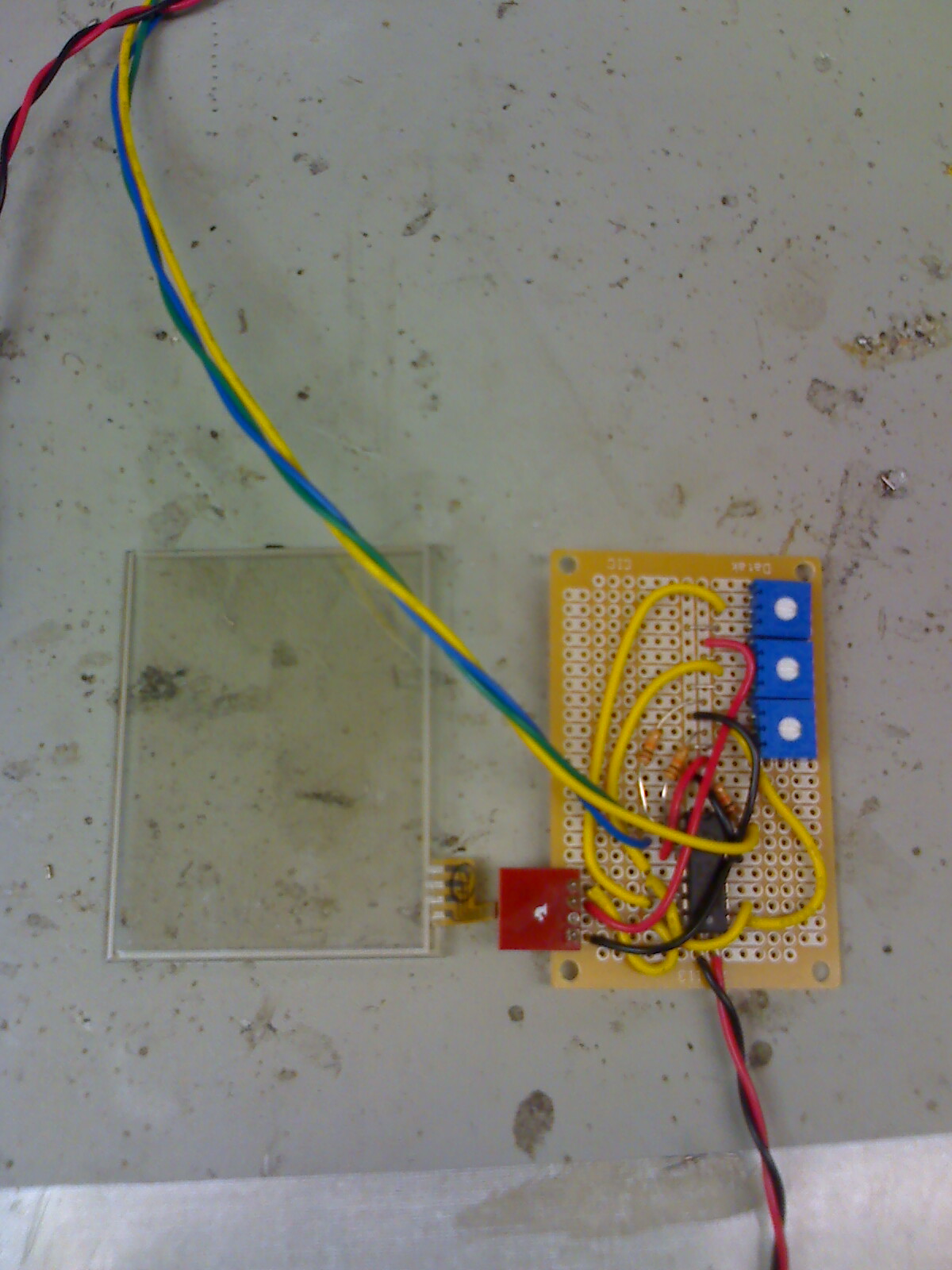
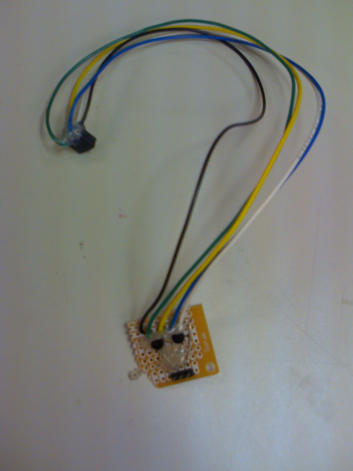
The circuit was contructed using the LM339, which has 4 comparators
with a common power input, and 3 potentiometers to set the three screen
regions. Three 10K pull-up resistors are required at the output of
each comparator. Red wire is connected to the power supply, black is
connected to ground, and green, blue, and yellow are connected to the
comparator outputs.
After constructing the touch screen circuit, I moved on to the PS/2
interface circuit, which just uses 2 BJTs (one for data and one for
clock) to interface the microcontroller to the 5V logic within the
computer PS/2 port. The base of the BJT connects to the
microcontroller output pin, and allows the microcontroller to pull the
signal low. The input pins connected directly to the PS/2 port are 5V
tollerant. The pull-up resistor is internal to the computer, so it is
not necessary on our interface.
The black wire is connected to ground, and the 3-pin header interfaces
to the PS/2 cable, which consists of clock, data, and the shielding
(ground). For simplicity, the 6-pin header for signal and ground
wires was aranged to connect to pins 19-24 on the mainboard's 24-pin
header (ground being pin 24).
April 26 (8 hours):
Today we did some
trouble shooting on the keyboard PCB. The code to read the state
of the keyboard is working, but the H-key is tied high as seen below.
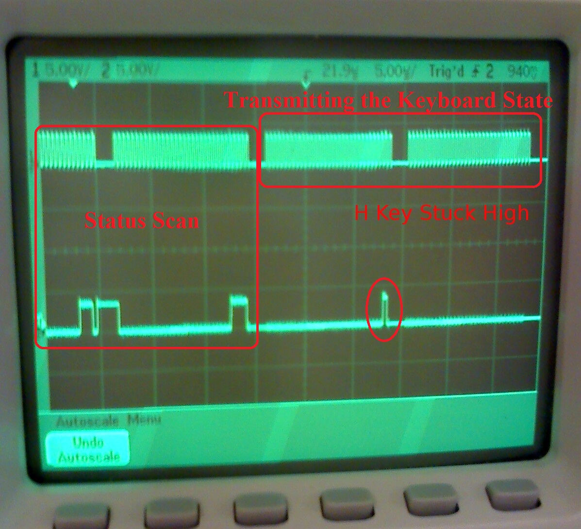
After pulling several pushbuttons off of the board, I discovered that
the signal trace was being shorted to one of the power pads on an
adjacent switch through a solder bridge. After a few failed
attempts to remove the bridge and solder the pushbutton back on, we
decided to just cut the signal trace and flywire around the damaged
trace. The solder mask had been damaged, and due to the close
proximity of the trace and power pad, it would have been very difficult
to stop the solder from flowing between the two.
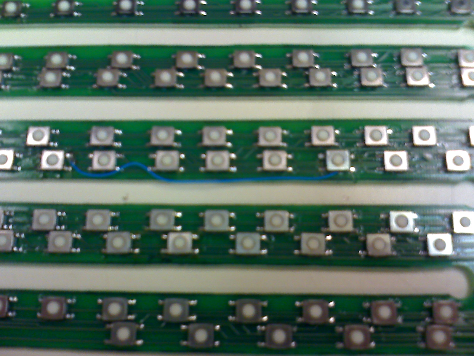
The signal traces for the C and V keys, and the M and comma keys were
also shorted to each other. This problem has yet to be solved but
can be taken into account in the code. Chuck helped us trouble
shoot the problem by removing the shift register and resistor pack, and
after removing both pushbuttons as well, the problem remained. No
solder bridges were found or damaged traces.
I then marked up the Plexiglas for all of our keys and Chuck began
cutting them on the shear. Once the remaining shorts on the key
signals are found we can glue all of the keys to the board.
April 27 (3 hours):
Last night Luke and
Dhruv discovered that the X and Y axes on the DS touch screen were
flipped, so the X and Y axis connections had to be flipped on the
circuit. I updated the touch screen schematic to reflect this and
added the pull-up resistors for a more accurate record of the circuit.

We will be switching between English, Greek, Russian for our
demonstration, so I first created a unicode chart to be inserted into
the code for the Russian keyboard characters using this Cyrillic Unicode chart(link).
I then finished cutting out the 61 plastic keys to be glued to the
keyboard. We then connected the keyboard and PS/2 interface to
the microcontroller development board, and began debugging the latest
code to use the keyboard to send characters directly to the computer,
which was successfully done by the end of the night.
April 28 (7 hours):
Today's focus was on
creating detailed documentation of the packaging design with dimensions
accurate enough to create all of the cutouts and holes required for
mounting all of the components. I started by laying out the
components from the top view, looking down at the keyboard and
screen. The following is the result:

The mainboard will be placed beneath the monitor in the cavity where
the monitor stand used to be attached. In order for this to work,
the monitor must be installed after the mainboard is already in place,
so the monitor must be mounted 1/2" from the left edge to slip past the
1/2" lip around the top of the case when being mounted. The
monitor must also be pressed tightly against the top of the case to
make as much room for the mainboard and cables as possible. The
touch screen and circuit will be placed in the upper right corner of
the screen, and the keyboard PCB will be placed in the lower right
corner. The keyboard keys have a 9"x5" viewable area when
packaged, and the touchscreen has a 2"x2" viewable area when packaged,
so the plastic faceplate will only have these two cutouts. Foam
rubber will be placed between the monitor screen and the keyboard and
touch circuit. The foam rubber will be cut thick enough to clamp
the two boards between the monitor and the plastic face plate and hold
them in place using friction. Small amounts of adhesive will be
applied if friction alone proves to be insufficient.
On the front view of the case, the cavity for the mainboard is
indicated along with the location of the mainboard and SD card. A
slot will need to be cut in the aluminum for the SD card, which will be
done using a jigsaw.

The location of the power supply card is also indicated for reference.
On the right side of the case, the AC power plug will be mounted along
with the power switch for the entire unit. Mounting holes for the
power supply board are also indicated.

On the bottom of the case, mounting holes will be drilled for the
mainboard, and the monitor also has four mounting holes on the back,
which I will utilize to secure the monitor if I can find the
appropriate screws.
April 29 (10 hours):
The goal for today was to make all of the cutouts in the project
packaging. I cut all of the square cutouts in both the plastic
faceplate and the aluminum case using a jigsaw, and I used a drill
press for all of the mounting holes. I used self-tapping screws to
create the threads in the aluminum for securing the faceplate to the
case.
Top View:

Front View:

Right Side View:

Internal Mounting Holes:

Later in the evening, I helped Luke and Dhruv troubleshoot the PS/2
implementation on the mainboard. It works correctly on the development
board but fails on the mainboard. After hours of troubleshooting and
searching through the code for errors, we determined that the
microcontroller functions correctly when the PS/2 interface circuit is
not attached, but as soon as the interface circuit is attached to the
microcontroller pins, the clock and data output pins on the
microcontroller output a nearly constant 0.8V. The load of the BJTs is
causing the microcontroller to malfunction, so the BJTs are most likely
not biased in the correct operating region. If this is the problem, it
does not explain why the circuit works when interfaced to the
development board.
April 30 (3 hours):
After researching BJT
characteristics and looking over the 2N3704 datasheet, I learned the
following. The transistor has a Vbe-on = 0.6V which explains why
the clock and data pins where stuck at around 1V. Also, the gain
is around 200, so assuming the PS/2 host (computer) has a pull-up
resistor of around 10K, the BJT should be biased for a collector
current Ic=5mA, resulting in the following bias circuit:
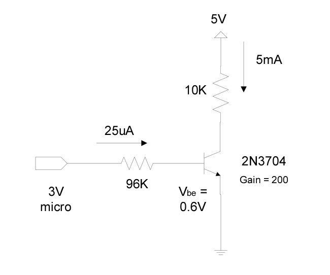
In the lab, a 91K resistor was the closest value available. Once
the resistors were added to the circuit, the PS/2 interface began
working, just as it did on the development board.
WEEK 16 SUMMARY
Accomplishments: This past week, the PS/2 interface circuit was
constructed and designed to connect to the 24-pin header on the
mainboard since it requires 4 microcontroller pins and a different
touch screen is now being used. After testing and debugging with
both the development board and mainboard, it was discovered that a
gross oversite was made by neglecting to place resistors between the
microcontroller pin and the base pins of the transistors. The new
touch screen control circuit was also constructed and tested. The
code for reading the state of the keyboard was debugged, and we
determined that one of the keys was shorted to power (h), and two pairs
of keys were shorted together (comma -> m and c -> v). With
Chuck's help, we found the short for 'h', but we were unable to find
the others without making potentially damaging actions. The
cutouts for the packaging were also made, and some of the components
were mounted to the frame. At the end of the week, three PSSCs
were functioning together on the mainboard and were checked off by
Malek.
Weekly Work Total: 39 hours
Project Work Total: 230 hours
Week 17
May 2 (4 hours):
Luke and I worked on
debugging the SD card on the mainboard. It worked correctly on
the development board, but when ported to the mainboard, it
failed. We narrowed down the point of failure in the code by
setting flags in the code and setting the oscilloscope to trigger on
the flag. Using this method, we determined that the SPI port was
not communicating with the SD card, so we removed the card and probed
the SPI signals directly. Doing this we found that the MISO pin
connected to the SD card slot on the motherboard was not working, even
when programmed as a GPIO pin and set to toggle. After setting
the pin to toggle at a very low frequency, however, we noticed that the
waveform resembled that of a cold solder joint. After adding
solder to the microcontroller pin, the MISO pin began toggling
correctly on the SD card slot. Luke then discovered, however,
that the code was not designed to address any more than two SPI ports,
and our microcontroller has four. So, since the SD card is on SPI
channel 3, the libraries themselves will need to be modified.
WEEK 17 SUMMARY
Accomplishments:
Weekly Work Total: 4 hours
Project Work Total: 234 hours