Purdue SoCET
About
The goal of Purdue SoCet (system-on-chip extension technologies) is to provide students hands on experience with a fully developed industry quality SoC design flow. Members of the group engage with architecture exploration, RTL design, physical design, PCB design, chip bringup, verification methods, an array of EDA tools and software development.
Recent tape-outs
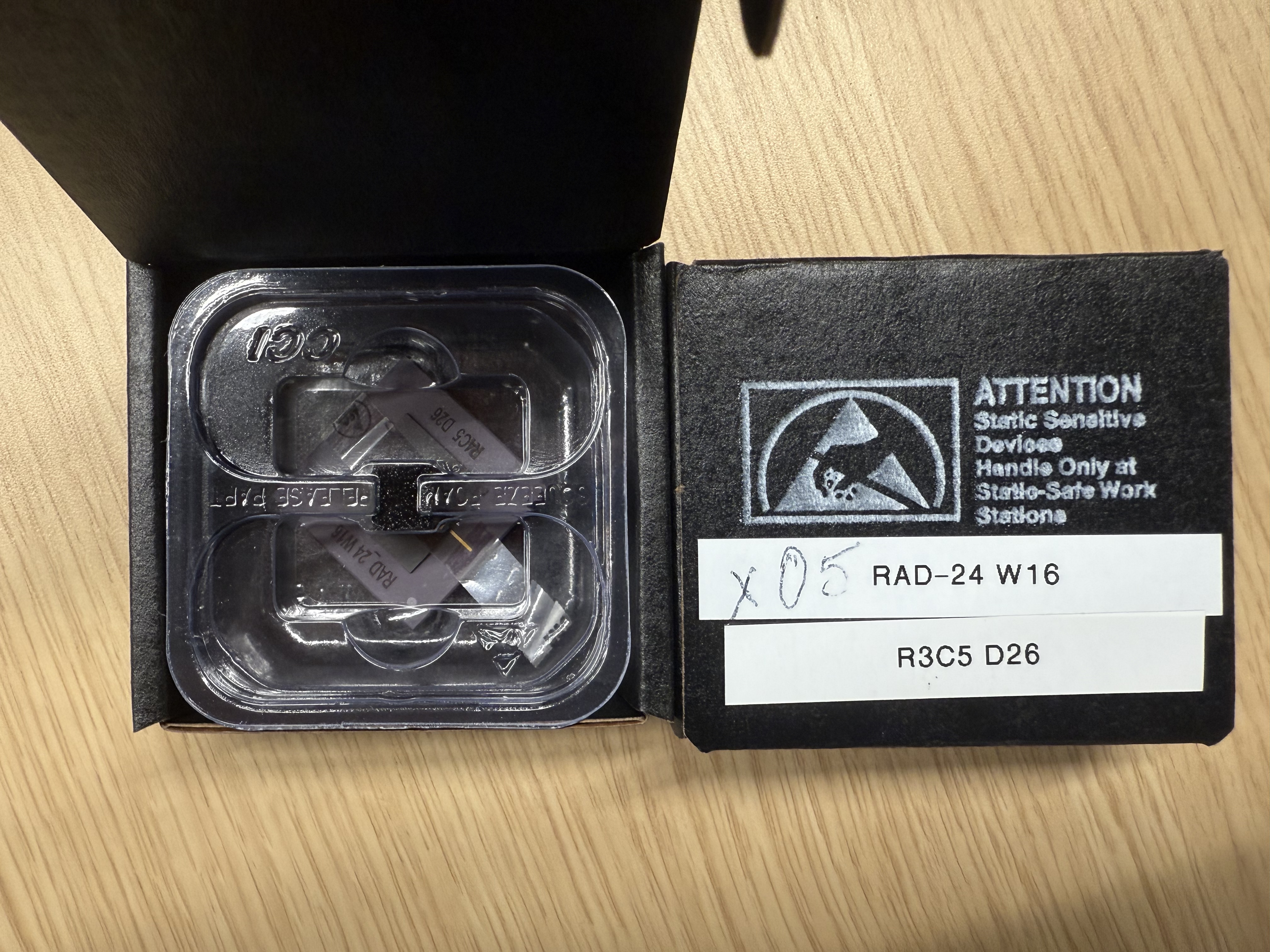
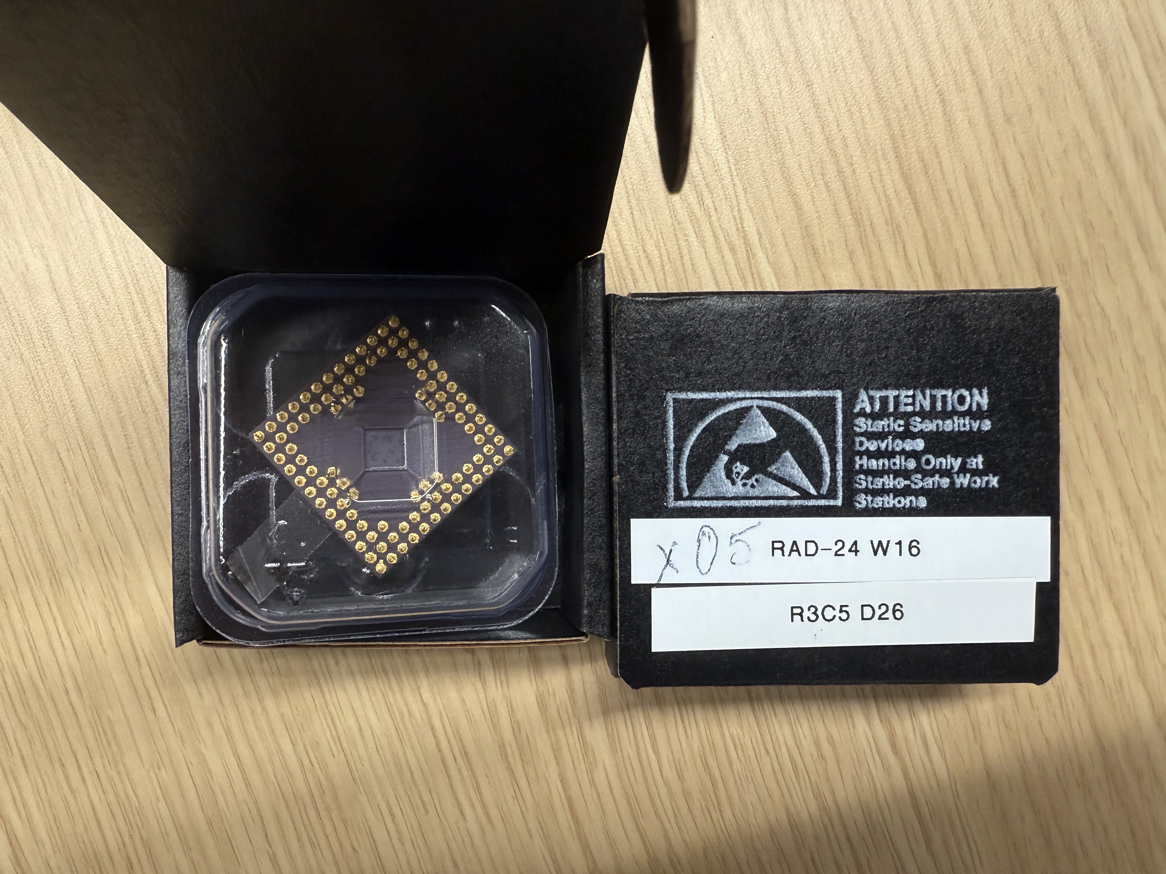
AFTx07+ 2024 for fabrication on the Skywater 130nm process. Preparing to be packaged .
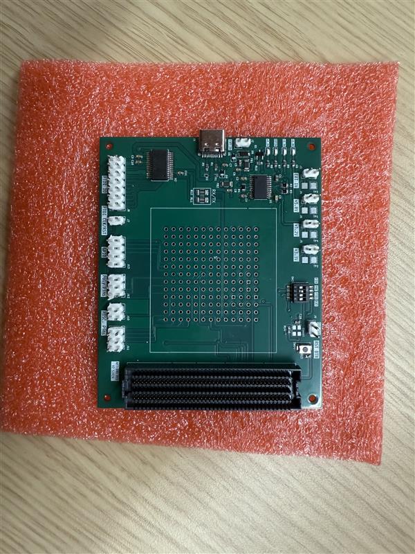
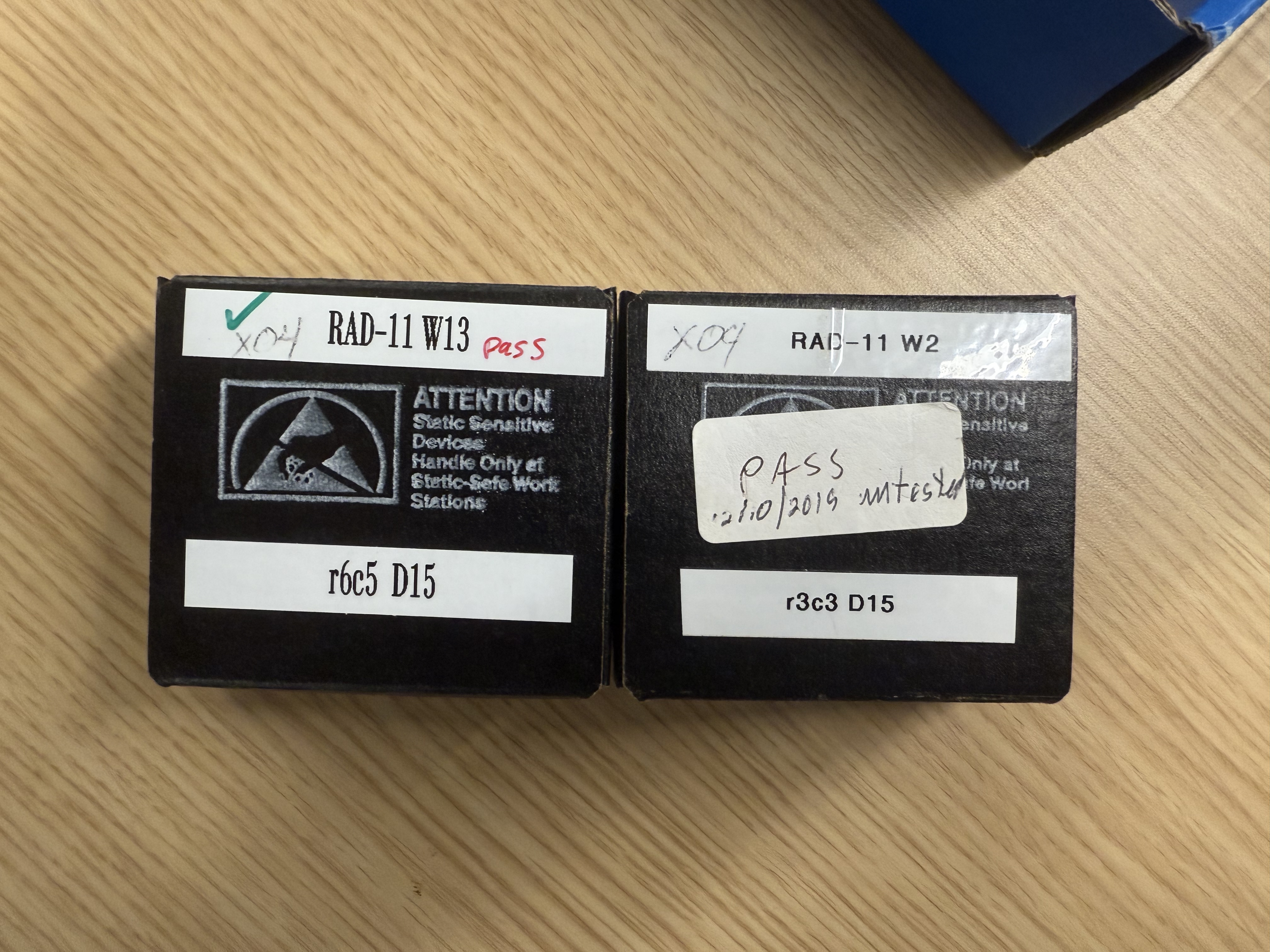
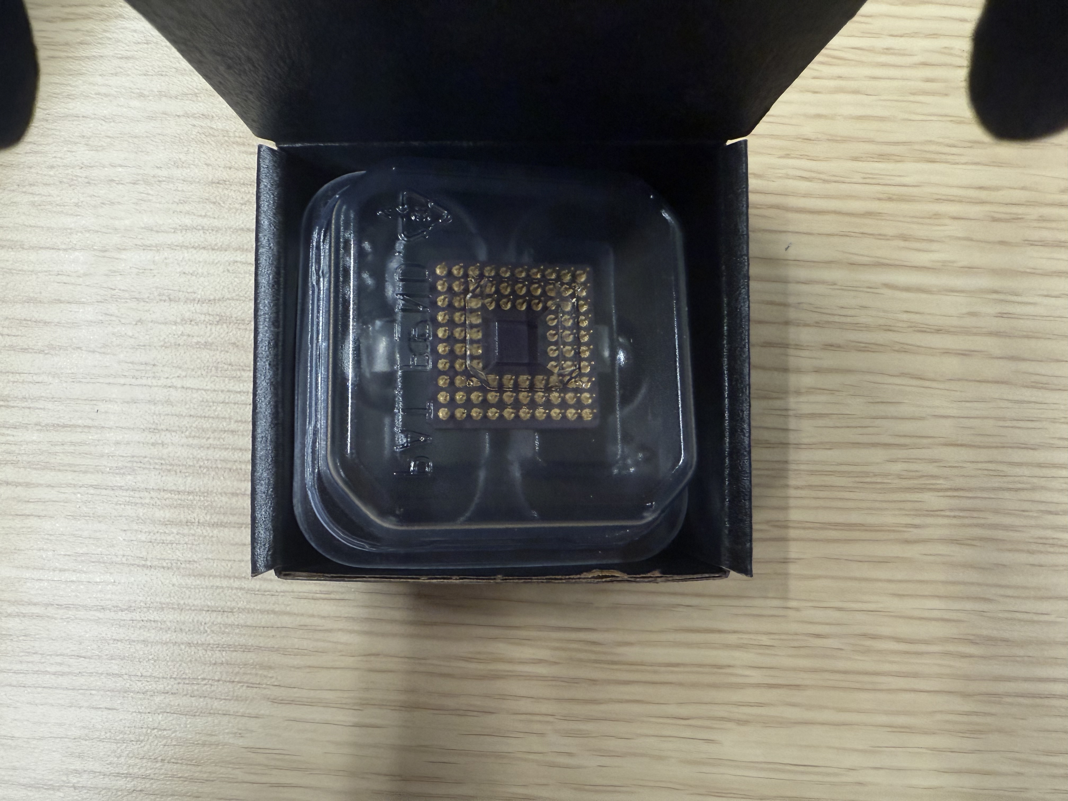
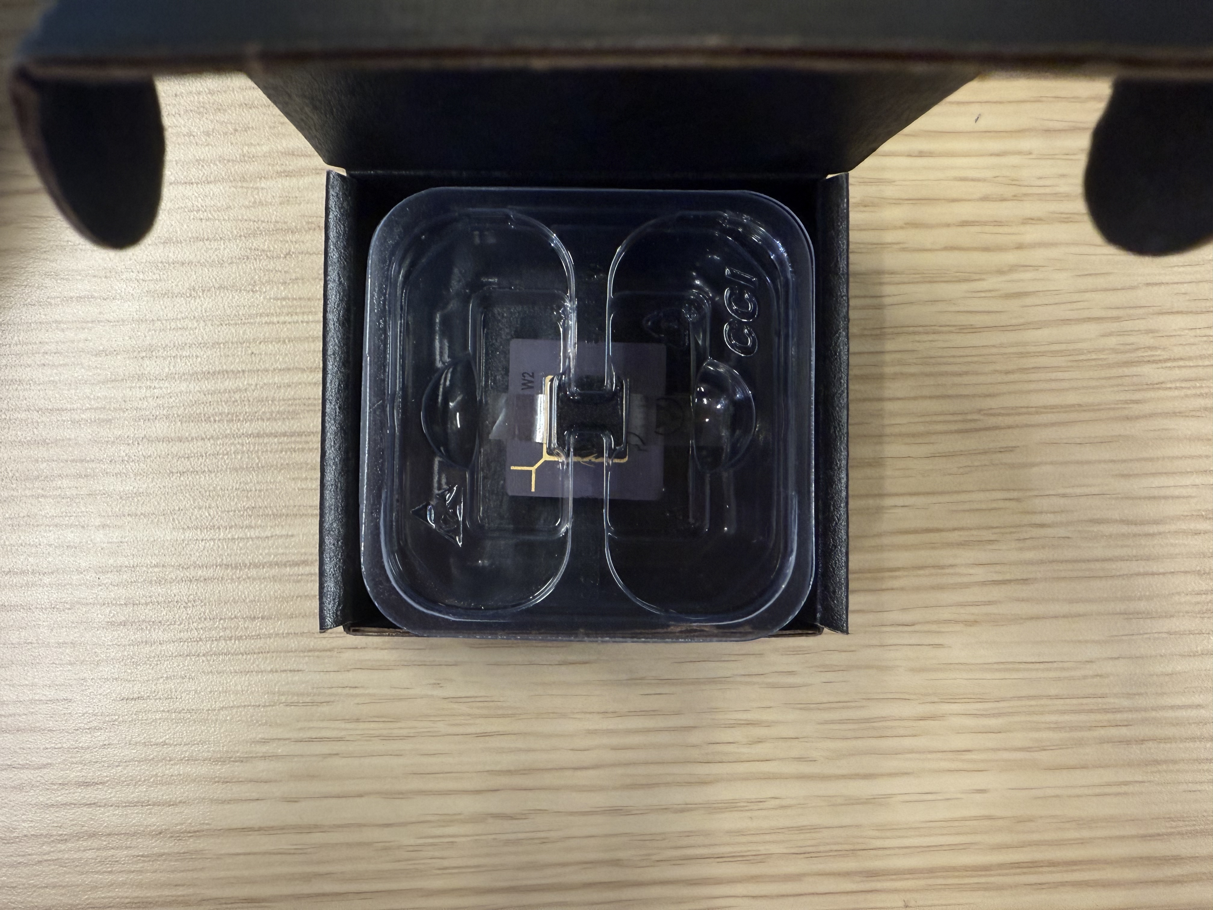
AFTx07 2024 for fabrication on the Skywater 130nm process. Bringup in progress.
2022: an experimental design on TSMC 180nm was taped out via MUSE Semiconductor. This IC is a test chip to demonstrate applications of polymorphic logic in logic locking, recongurability, and countermeasures against reverse engineering.
AFTx06 2021 for fabrication on the Skywater 130nm process in connection with the Google sponsored open-source MPW runs as described here.
Announcement
Summer and fall application forms now available
- If you are a freshman or sophomore or have minimal background in electronics or microcontroller programming, please apply for STARS/Intro to SoCET.
- If you have already completed courses such as ECE 20007 and ECE 27000 or you have other significant electronics experience, please apply to be part of the main SoCET team in Spring 2026. Main Team SoCET Fall 2026 application form
See Team Brochure for descriptions of subteam and project opportunities.
Application deadlines
- March 13 end of day - for VIP pre-registration for the fall, or for an early decision on acceptance for summer. Decisions to be announced March 25.
- April 24 end of day - for open registration for the fall or summer. Decisions to be announced by May 12.
- August 14 end of day - last chance to apply for fall. Decisions to be announced by August 21
If you need more information about SoCET and how to join the team, please email socet@purdue.edu.
System-on-Chips
Items on Roadmap for AFTx07 and Later
- 6 stage RISCV pipeline created
- Vector extension to RISCV CPU
- ISA extensions: atomic, compressed, floating point, privileged
- Developing an LLVM based compiler to exploit the sparsity optimizations in our current RISCV core.
- Adding support for RUST programming language
- freeRTOS
- FPGA prototyping of our design with an eye to using it as a software development platform for our design.
- Multi-core
- L1/L2 cache
- Multi-core interrupts
- Branch predictor
- RISCV verification
- RISCV debug
- DMA controller
- Power management
Other projects and collaborations
- Several analog mixed signal student projects including a low drop-out regulator, op-amp, DAC, and adding wireless support to a future version of our chip, as part of a collaboration with the HINET lab.
- GPU accelerator design - T Rogers
- Reverse engineering countermeasures - J Appenzeller
- MRAM hardware security - J Appenzeller
- Spectral Analsys for space observatory – T. Jamieson-Hooks, Arizona State University
- FPGA fabric synthesis – A. Lukefahr, Indiana University
Details on older versions of the AFTx chip can be found here.
GPU Team
- Develop SIMT (Single Instruction, Multiple Threads) GPU targeting graphics and parallel workloads
- Full-stack GPU design following industry standards: workloads, software stack, custom ISA, compiler, architecture, simulation, and RTL
- End-to-end development from applications and kernels down to cycle-accurate models and RTL
- Split into: graphics & software, compilers, hardware architecture & RTL
AI Hardware Team
- Develop AI accelerator for both training and inference
- Full software–hardware stack: PyTorch kernels, system software, compiler, architecture, and RTL
- Focus on performance, efficiency, and scalability through hardware–software co-design
- Split into: system software, compilers, vector core, scheduler, systolic array, scratchpad, and DRAM/memory
Data Center Network Accelerator
- Develop a network accelerator for datacenter and distributed systems workloads.
- Full-stack design: networking stack, software, architecture, and RTL
- Focus on high throughput, low latency, and scalable data movement
Digital Design
- Focuses on the architecture and implementation of RISC-V–based systems and advanced SoC components
- Projects span improvements to the RISC-V CPU core, work on the chip interconnect, and development of digital peripherals.
- Example RISC-V projects: Multi-core processor, multi-core interrupts, RISC-V extensions, branch predictors, DMA, power management
- Example peripheral projects: SPI, PWM, Timer
Verification
- Ensures correctness and reliability of SoC designs
- Focuses on industry standard UVM-based verification and reusable testbenches
- Validates processors, memory systems, and custom hardware blocks
Analog/Mixed Signal
- Focuses on designing non-digital components that bridge real-world signals and on-chip processing
- Enables integration between physical sensors, power systems, communication interfaces, and digital logic
- Example projects: LDO, Op-amp, DAC, Wireless
Software
- Compiler toolchains, IO libraries, RTOS porting, demo applications
Physical Design
- Open-source and commercial synthesis/layout/verification
- Physical verification: power and timing
- Tape-out preparation
PCB/Test
- PCB designs for testing and IC demonstrations
Test Engineering
- DFT, ATPG, and post-silicon validation
Papers
M.C. Johnson. ASSURE Final Report. Aug 2020.
J. Covey, M. C. Johnson – System-on-a-Chip Design as a Platform for Teaching Design and Design Flow Integration, Proceedings of the 2019 on Great Lakes Symposium on VLSI, Tysons Corner, VA, 2019.
J. R, Stevens, J. Skubic, E. Colter, and Dr. M. Swabey. Purdue microbrewer: A microcontroller generator. RISCV Microelectronics Conference 2017, Mar 2017.
J. Skubic, J. R. Stevens, C. Y. Tan, Dr. M. Johnson, and Dr. M. Swabey. Riscv-business: A configurable, extensible risc-v core. RISCV Microelectronics Conference 2017, Mar 2017.
M. A. Swabey and M. C. Johnson. Satisfying ABET criterion using an industrial microelectronic skills incubator. 2015 IEEE International Conference on Microelectronics Systems Education, May 2015.

