|
|
|
Prof. Xu’s laboratories house state-of-the-art facilities
including ultrafast laser systems and characterization equipment.
The majority of Prof. Xu’s research facilities are located
in the Birck
Nanotechnology Center, with some in the building of the
School of Mechanical Engineering.
 |
- Four ultrafast femtosecond
pulsed laser systems used for energy transfer
diagnostics, nanomanufacturing, and material
synthesis
- Three femotosecond
laser-based 3D nanoprinter
- High precision femtosecond
laser micro-machining workstation
- Nanolithography system using
optical antenna array
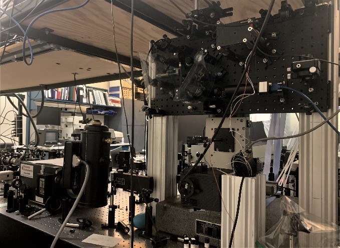
Image on the left shows our
continuous, rapid multiphoton projection 3D printing
system.
|
- Two optical paramatric
amplifiers, wavelength tunable from UV to IR
- Pump-probe lines for
femtosecond time-resolved measurements including
TDTR
- Temporal pulse shapers for
pulse shaping and coherent control studies
- Nanosecond laser thermal
reflectance measurement apparatus for measuring
thermal conductivity and contact resistance
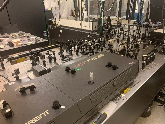
Image on the right shows our
ultrafast time-domain thermoreflectance system for
thermal characterization of materials.
|
 |
- Chemical vapor deposition
(CVD) system for growing silicon nanowires and
carbon-based nanomaterials
- Home-built AFM and NSOM with
wavelength extended to near-IR (~1.8 micrometers)
and coupled to FTIR
- Fourier Transfer Infrared
(FTIR) Spectrometer, coupled with an IR microscope
- Other equipment such as a
Raman Microscope, single shot auto-correlator,
lock-in amplifiers, shakers, etc.
- Computational facilities
including small clusters in the group and access to
Purdue central computational
- A test rig for testing the
performace of thermoelectric generator (TEG)
|
|
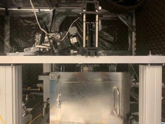
Nanoscale radiation apparatus
|

Near-field scanning optical
microscope (NSOM)
|

Fourier Transform Infrared
(FTIR) Microscopy
|

Raman Spectrometer (LabRAM800)
|
Group members have access to the clean-room micro/nano fabrication
and characterization facilities in the Purdue Birck Nanotechnology
Center, including focused ion beam (FIB), electron beam lithography,
SEM, and TEM.
|