Frontiers
WINTER 2026
Industry Partnerships

Google collaboration positions Purdue at forefront of AI-driven innovation
January 15, 2026
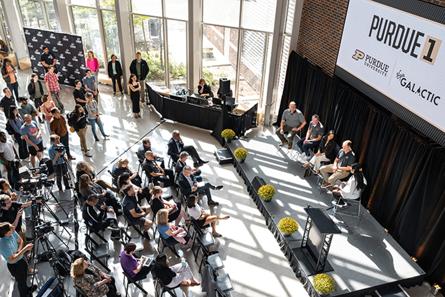
All-Boilermaker team to crew Virgin Galactic suborbital mission Purdue 1
January 14, 2026
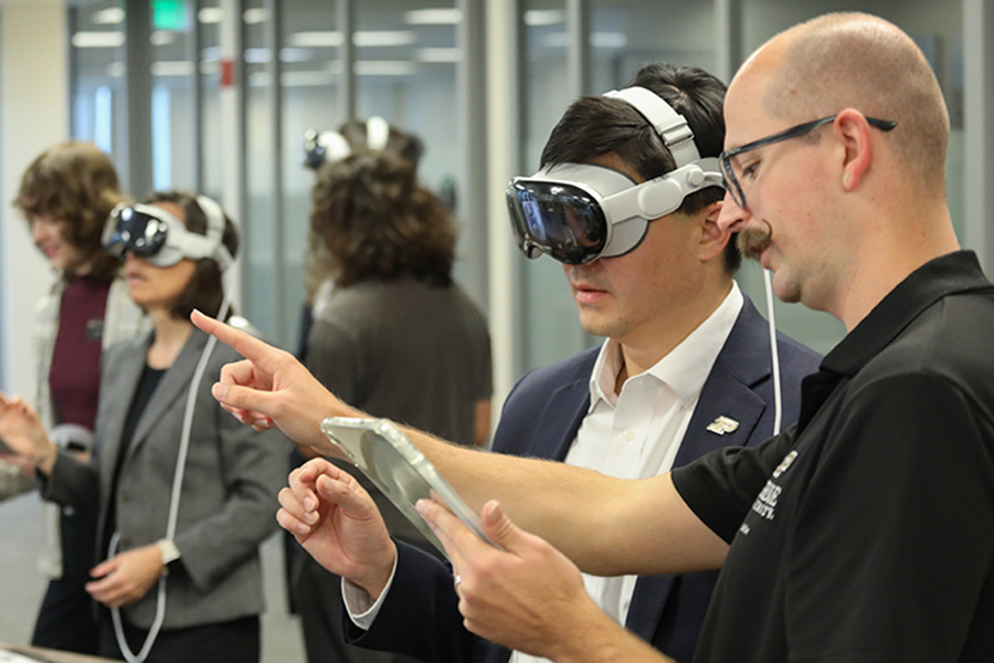
Apple Computing Hub prepares next-gen innovators
January 13, 2026
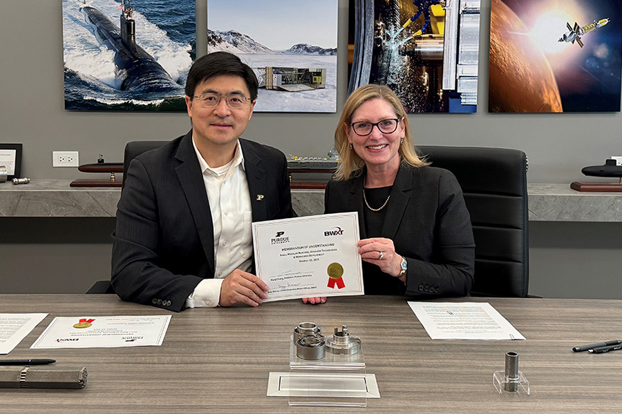
BWXT and Purdue forge strategic collaboration to advance nuclear innovation
January 12, 2026
Rolls-Royce & Purdue Safeguard the Future
January 11, 2026
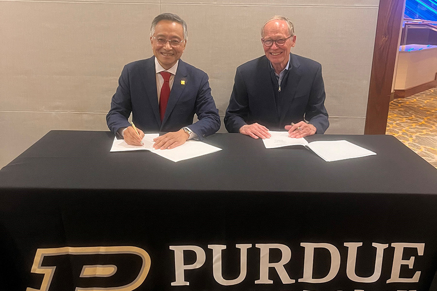
Purdue and ASML partner to advance semiconductor R&D, grow industry workforce
January 10, 2026
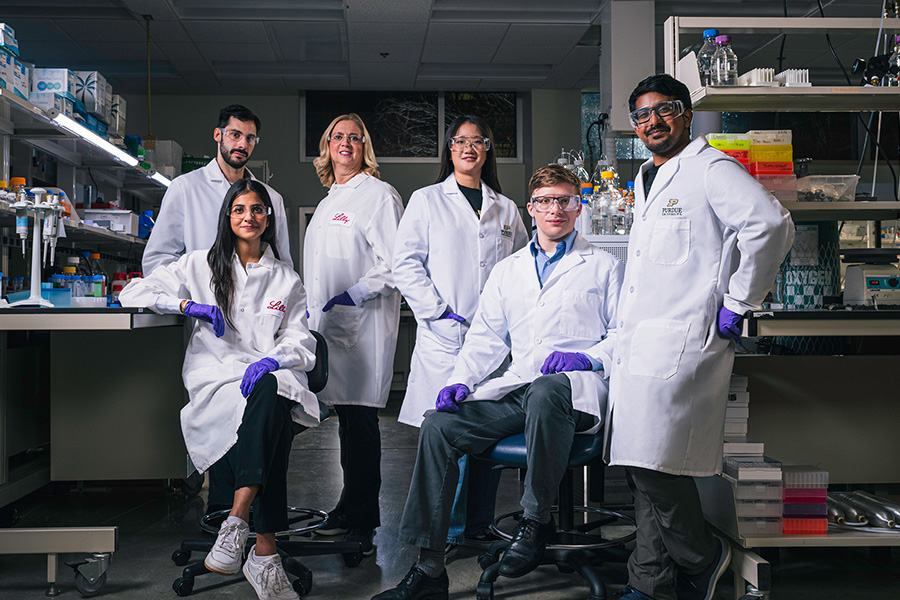
Lilly shares Purdue mission to improve lives worldwide
January 09, 2026
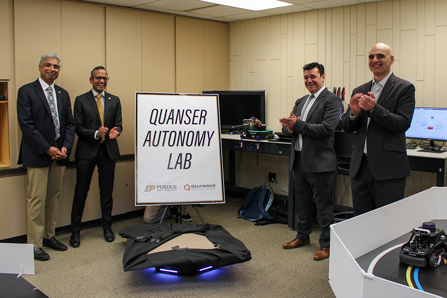
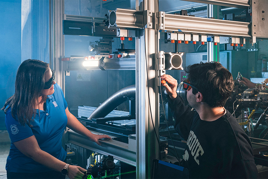
Quanser helps to expand autonomous and connected systems education for engineering students
January 08, 2026
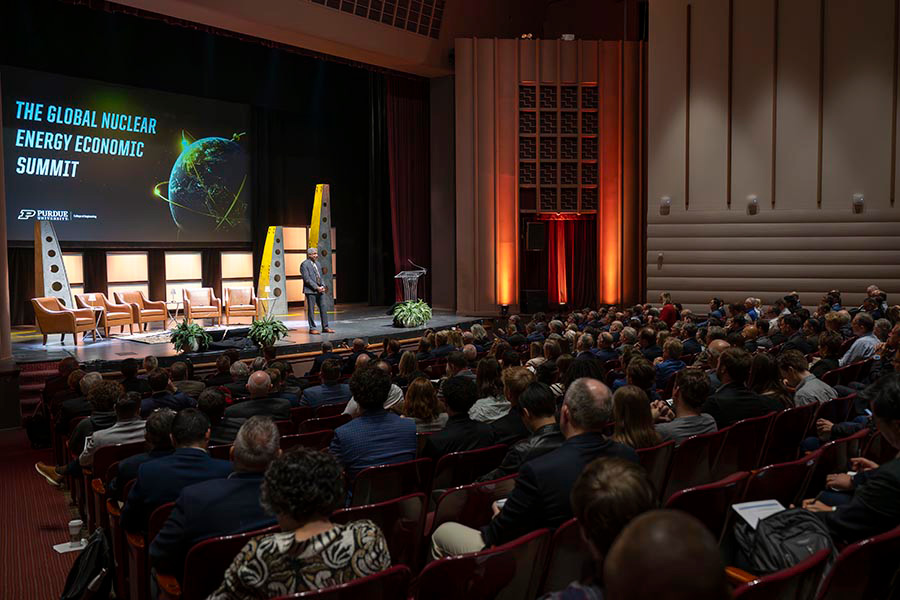
Global Nuclear Energy Economic Summit advances Indiana's role in nuclear innovation
January 06, 2026
Purdue emerges as America's leading institution in manufacturing and supply chain
January 05, 2026
Advancing innovation for supply chain resilience
January 02, 2026
Space Force partnerships open new research, graduate opportunities
January 01, 2026
Educational Innovations
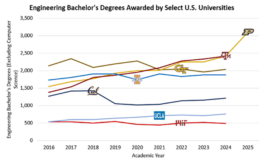
Purdue Engineering emerges as the national leader in degrees awarded and market demand
January 03, 2026
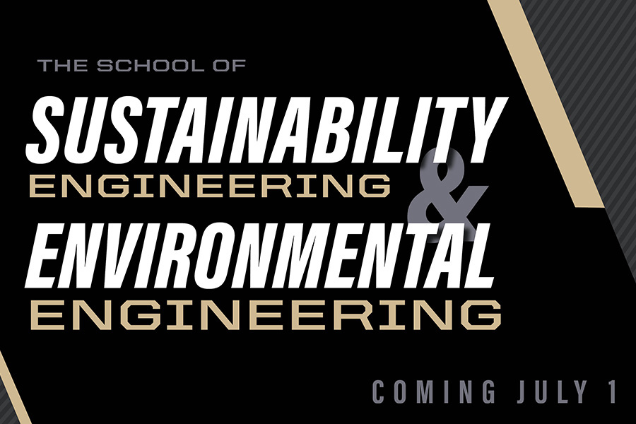
Purdue launches School of Sustainability Engineering and Environmental Engineering to meet growing industry demand
January 02, 2026

Space systems degrees program meets the challenge of modern engineering
January 01, 2026
Purdue launches nation's first online credential program in small modular reactors
December 31, 2025
Purdue first to establish AI graduation requirement
December 22, 2025

Springer Business Initiative expands business essentials certificate for Purdue Engineering students
December 21, 2025
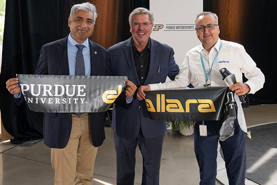
Dallara and Purdue Motorsports celebrate transformational partnership
December 20, 2025
Organizational Developments


Frontiers | Fall 2024
Previous IssuePurdue Engineering powers Vision 2030 — aiming to be the nation’s #1 impactful engineering college. Celebrating 150 years, FRONTIERS highlights: leading the $1B SMART USA digital twin semiconductor institute, new CHIPS & AI Institute, major manufacturing & industry wins, top rankings & more.