As semiconductor device sizes shrink, chip design software is increasingly flying blind. With nanoscale-sized components, performance often hinges on the precise arrangement of atoms and the predictable behavior of electrons or phonons (vibrations) passing through their atomic structures. Yet, today’s commercial device design software treats matter as a continuum and views electrons only as classical particles.
“The number of atoms in today’s transistors are so small they have become countable,” says Gerhard Klimeck, director of the Network for Computational Nanotechnology, Reilly Director of the Center for Predictive Materials and Devices, and professor of electrical and computer engineering. The 22nm-nanometer fabricated Intel transistors that fuel entry-level desktop computers, for example, have silicon feature sizes that are only 8nm thick and 64 atoms wide. With the latest 14nm and 10nm transistors, some critical layer thicknesses are as small as 10 atoms.
“Today’s CAD tools are almost all agnostic of the existence of atoms — they describe atoms as ‘a continuum matter,’” says Klimeck, who is also the Reilly Director of Purdue’s Center for Predictive Materials and Devices (c-PRIMED). “That’s where our NEMO simulation engine comes into play. By using atoms as the representation basis, we can construct objects one atom at a time.”
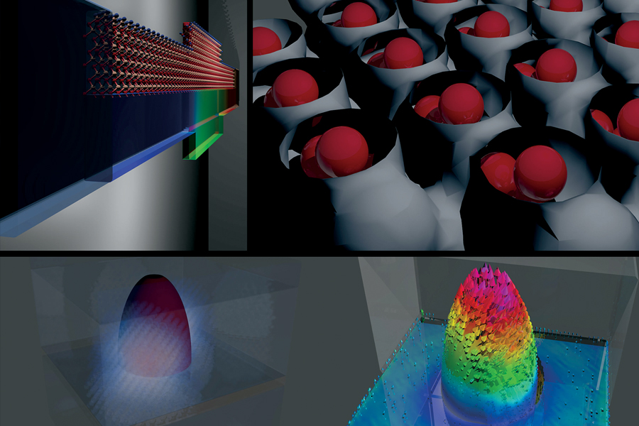
The latest NEMO (NanoElectronics MOdeling Tools) simulation engine — NEMO5 — is notable for providing atomic-resolution calculation of nanostructure properties. NEMO5 “treats electrons fully quantum mechanically,” says Klimeck.
Modified versions of NEMO5 power nine simulation tools available to academics and students on a Purdue-hosted, National Science Foundation-funded website and simulation platform called nanoHUB.org that Klimeck helped establish and now directs. The open access site offers browser-based control of some 500 applications and over 5,000 content items used by 1.4 million academics and students annually.
Founding NEMO
NEMO — as well as nanoelectronics research in general — was inspired by the work of Klimeck’s Purdue advisor, Supriyo Datta, “who was at the forefront of research into quantum transport,” says Klimeck. Datta is the Thomas Duncan Distinguished Professor of Electrical and Computer Engineering.
After graduating with a PhD in 1994, Klimeck worked in a Texas Instruments R&D group, where he was part of a small team that built the first-gen NEMO. The software was the first industrial simulation tool based on nonequilibrium Green’s functions that could quantitatively and predictively model certain types of quantum devices, such as resonant-tunneling diodes.
In 1998, Klimeck went to work at NASA, where he built application code for the world’s first parallel cluster computers. He also developed a 3D version of NEMO. “With NEMO-3D, we could model in three dimensions,” says Klimeck. “However, unlike NEMO-1D, it could not model the electron flow because it was computationally too demanding to do both. When I came to Purdue in 2003, we began to combine these two concepts into new toolsets that evolved into NEMO5. With NEMO5, we can combine electron flow and structure modeling in one, two and three dimensions for electrons, photons and phonons, which reveal thermal flow.”
The 3D modeling capabilities enabled by NEMO3D and NEMO5 go far beyond fundamental ab-initio computational material science methods, which are typically limited to about 100 atoms and limited to equilibrium material properties. “Our realistic devices are much larger and operate far from equilibrium,” says Klimeck. “We extract the critical essence of electronic structure from these fundamental codes, and then scale the problem size to realistically extended devices.” Supported calculations include strain relaxation, phonon modes, electronic structure using the tight-binding model, self-consistent Schroedinger-Poisson, and quantum transport.
“Circuit-level design needs very good descriptions of device behavior without simulating the physical processes in the devices,” explains Klimeck. “This is expressed in so-called compact models, which enable a few parameters to determine how a certain class of transistors behaves within a circuit.”
Compact model formulas enable designers to “pick and choose some classes within the circuit,” but they fall far short of fully characterizing it, says Klimeck. “To get to parameters that characterize transistors or evaluate different transistor designs or different geometries, you need transistor-level 3D representations, with all materials involved at all the gates.”
Such a 3D representation is beyond the capability of simple analytical formulas, says Klimeck. “You need to find the coefficients of those parameters, which you can only do through costly experiments or by using a simulation engine like NEMO that lets you explore classes of devices at the atomic level.”
A Boon for Exotic Materials Research
NEMO5 is especially useful when researchers move beyond well-known materials and geometries, such as silicon or germanium, to work with exotic materials like III-V semiconductors or novel 2D materials. Such materials are being “intensively explored to augment the end-of-roadmap silicon devices,” says Klimeck. “The down-scaling of traditional silicon devices must stop at the physical end of countable atoms, so there is a global hunt for the next replacement switch in a new material system, as well as for alternative computing architectures. All these alternatives need to compete with the packing density and size of tomorrow’s silicon devices that are at the size scale of a few atoms. NEMO-like tools will be needed to explore those new worlds.”
For traditional materials, typical design tools — as well as NEMO — can “simulate things like a transistor’s current voltage characteristics or output characteristics,” says Klimeck. “But if you are working on the forefront of research into alternative materials, such as 2D layered materials or tunneling transistors that use III-V or gallium nitride, traditional tools fall short.”
NEMO, on the other hand, can model any semiconductor or metallic material, says Klimeck. “That’s because everything we do is fully quantum mechanical,” he adds. “If you have fluctuations or disorder in a device, we can automatically account for it. Most commercial tools treat electron flow in a classical sense, as if it were a fluid rather than a quantum mechanical wave.”
The NEMO5 engine that powers nine applications on nanoHUB offers a subset of the complete capability. “You need to be a computational expert to drive that Ferrari, so for nanoHUB, we give people the equivalent of a Volkswagen or Toyota to run predefined problem sets and problem spaces geared to certain classes of geometries such as nanowires. It’s still complex but not as complicated to use.”
NEMO’s research team has partnered with industrial sponsors that have begun to use the NEMO5 toolset internally for device designs and exploration. Tillmann Kubis, research assistant professor of electrical and computer engineering, has taken the lead in the technical developments of NEMO5 and reached an agreement with Silvaco Inc. to integrate NEMO capabilities into a commercial software pipeline. Purdue Research Foundation and Silvaco signed an agreement regarding NEMO on Aug. 24, 2018.