Capabilities
Versatile Crystal Structures
The main simulation object of NEMO5 is an atomic structure. In order to study it, it has to be created in the simulator. Currently NEMO5 is able to create pseudomorphically grown crystal structures only. The pseudomorphic growth assumes that all the materials that a device consists of have the same crystallographic structure. Variety of the heterostructures that can be considered as pseudomorphic is very large. It includes, e.g. GaAs/InAs/AlAs, GaN/InN/AlN, GaSb/InAn/AlSb structures and many others. In the future we will support also the non-pseudomorphic structures.Currently we support several crystallographic symmetry groups, such as simple-cubic, diamond, zincblende, wurtzite, trigonal structure of BiTe and graphene.
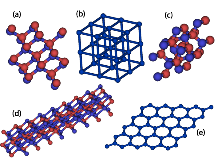
Different crystal structures that can be employed: a) zincblende. b) simple-cubic. c) wurtzite. d) trigonal. e) graphene.
Creation of the crystal structure is done as follows
In order to perform the simulation we need to know also the information about chemical bonds between the atoms. We assume that the atoms are chemically bound to their nearest neighbours only. The table of atomic bonds is created after the structure is built and stored for the subsequent usage.
Since the structure that we need to simulate can be too large to be stored and simulated on a single CPU, the structure builder can create the atomic structure in a distributed way on many CPUs in parallel. In this case each CPU stores both a small portion of atoms that belongs to him and the nearest neighbours of his atoms that belong to different CPUs. This tactics allows to distribute 100 million atom structure over a 100 thousand CPUs.
Additional features, that the crystal builder has, are:
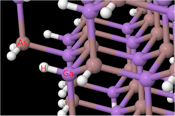
GaAs atomic structure with passivated dangling bonds.